Short Tutorial on PSpice
Spice is a
program developed by the EE Department at the
Using Spice is not very
intuitive to use because the input is an ASCII file rather than a circuit
diagram, and the output is another ASCII file rather than a graph. Several companies have developed graphical
user interfaces for Spice, which make it much easier to use. One of the most popular is PSpice. PSpice provides a free student version of its program which
can be downloaded from www.pspice.com.
To use PSpice,
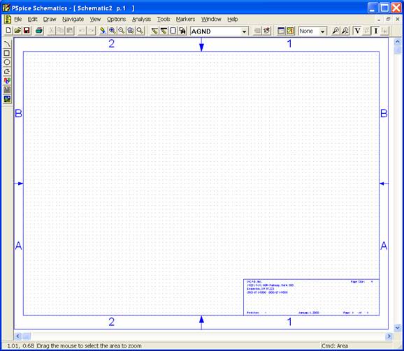
start with the PSpice Schematics program. When you
start up you will get a screen which looks like this:
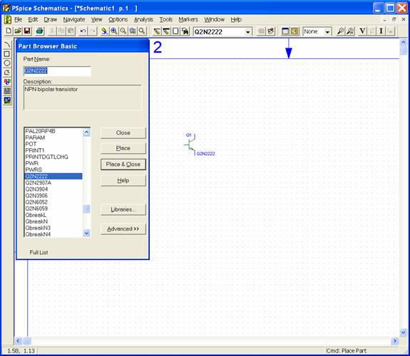
To put in a component, use
the Draw drop-down menu, and select Get new part (or use the shortcut
Ctrl-G). This will bring up a dialog box
which will allow you to select pats from libraries. If the part you want is not on the list, try
another library – parts such as transistors will probably be in eval.slb, while
things such as voltage sources will be in analog.slb. Select the part you want and place it on the
schematic:
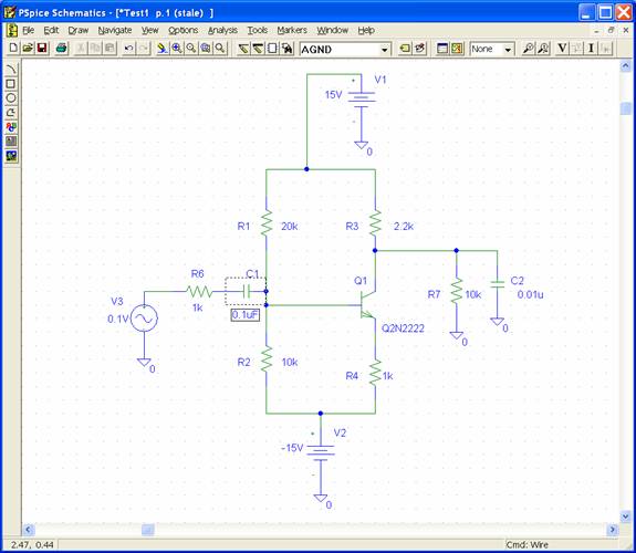
Continue placing the
components you need. (If
need a component of the same type as one you have already placed, you can use
the Draw – Place Part (Ctrl-P)
shortcut.) You can rotate an
object by clicking on it to highlight it, then use Edit – Rotate (or Ctrl-R). You can
change the value of a component by double-clicking on the component value, and
entering a new value. You can connect
components together by placing wires – Draw
– Wire (or Ctrl-W). Be sure to place
an analog ground (AGND). Use the component VDC for DC power supplies, and VAC
for signal sources. When done you will
have something which looks like this:
Be sure to save the file,
then go to Analysis – Setup. Here you will tell PSpice
what you want it to do. Always select Bias Point Detail. In this case we will also select AC Sweep which will give the frequency
response of the circuit.
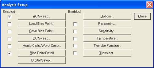
Click on AC Sweep to tell what frequency range
you want to use:
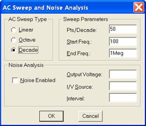
Here we will cover the
frequencies from 100 Hz to 1 MHz.
(Note: Use Meg for 106. If you use M, PSpice
will interpret this as milli (10-3).) Now choose Analysis – Simulate and PSpice will run,
and pop up an analysis window:
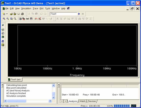
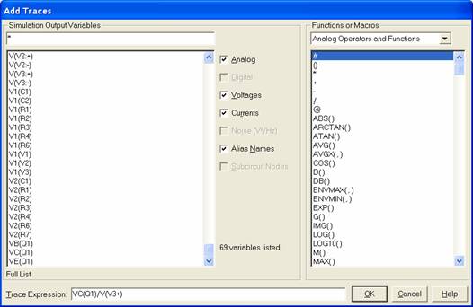
In this window choose Trace – Add Trace. Since we’re interested in the gain of the
circuit, we want to plot the output voltage divided by the input voltage. The output voltage is the voltage at the
collector of Q1, and the input
voltage is the voltage at the + terminal of V3,
so we plot VC(Q1)/V(V3+).
We now see the frequency
response plot:
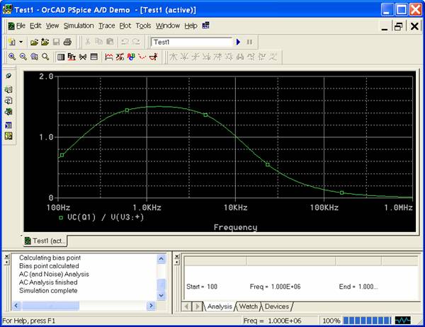
We see the circuit has a
gain of about 1.5 at a frequency of 1 kHz.
The theoretical value is about (RL
|| RC)/RE, or 1.8.
To see the bias voltages and
currents, you can look at the ASCII output file. However, it is easier to go back to the Schematic program and select Analysis – Display Results on Schematic
and then Enable Voltage Display
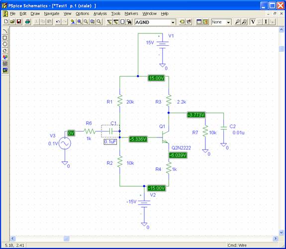
and/or Enable Current Display. Here is the schematic with the bias voltages
displayed:
It is instructive to look at
the ASCII output file. Here is part of
it:
Q_Q1 $N_0002 $N_0001 $N_0003 Q2N2222
R_R4 $N_0004 $N_0003 1k
R_R2 $N_0004 $N_0001 10k
C_C2 $N_0002 0 0.01u
V_V2 $N_0004 0 -15V
R_R6 $N_0006 $N_0005 1k
V_V3 $N_0006 0 DC 0V AC 0.1V
V_V1 $N_0007 0 15V
R_R1 $N_0001 $N_0007 20k
R_R3 $N_0002 $N_0007 2.2k
R_R7 0 $N_0002 10k
C_C1 $N_0005 $N_0001 0.1uF
This is the type of file
Spice needs – it shows that Q1 is a
2N2222 transistor, and its collector is connected to Node 2, its base to Node
1, and its emitter to Node 3.
Later on in the output file
we find the specifications for the 2N2222 transistor:
Q2N2222
NPN
IS
14.340000E-15
BF 255.9
NF
1
VAF
74.03
IKF
.2847
ISE
14.340000E-15
NE
1.307
BR
6.092
NR
1
RB
10
RC
1
CJE
22.010000E-12
MJE
.377
CJC
7.306000E-12
MJC
.3416
TF 411.100000E-12
XTF
3
VTF
1.7
ITF
.6
TR
46.910000E-09
XTB
1.5
CN
2.42
D
.87
The standard Spice model
assumes the 2N2222 has a b of 255.9. You can edit the transistor model if you want
to use a different value of b.
We can also see the bias
voltages at the nodes:
NODE VOLTAGE
NODE VOLTAGE
($N_0001) -5.3359 ($N_0002) -3.7732
($N_0003) -6.0390 ($N_0004) -15.0000
($N_0005) 0.0000 ($N_0006) 0.0000
($N_0007) 15.0000
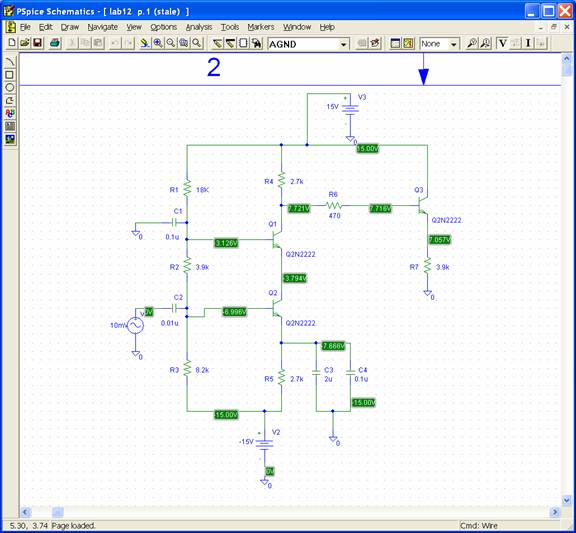
Here is the schematic for
the RF amplifier circuit of Lab 12:
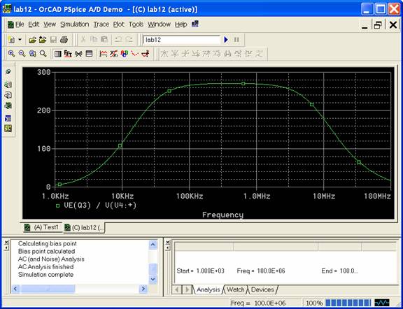
and the frequency response shows the passband
gain is about 280:
For some circuits the
transient response is more important.
For example, consider the CMOS inverter:
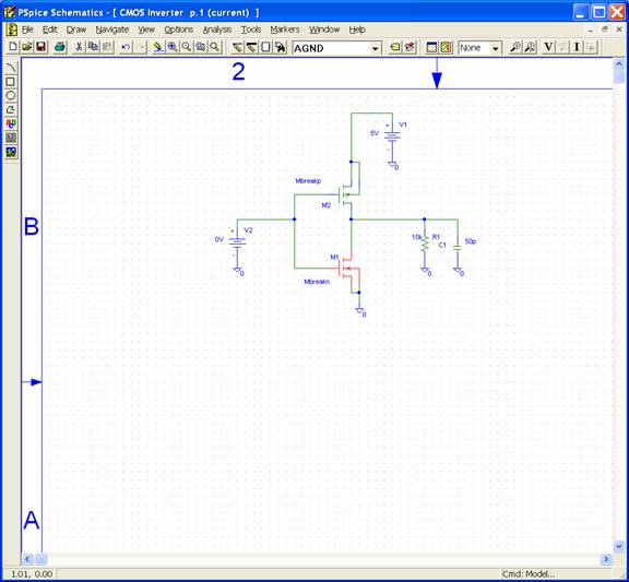
The MOSFET models are located in the breakout.slb library, under the names Mbreakn (NMOS) and Mbreakp (PMOS). We now need to define the parameters of the MOSFETS: highlight the NMOS transistor and select Edit – Model:
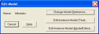
Select
Edit Instance Model (Text):
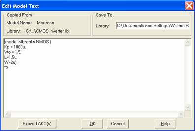
and enter appropriate values for the parameters. Here we have
kn’ = 100 mA/V2, Vt = 1.5 V, L = 1.5 mm, and W = 2 mm.
Do the same for the PMOS
transistor.
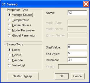
Now we will do a DC sweep
rather than an AC sweep. Choose Analysis – Setup, then
select DC Sweep. Sweep source V2 from 0V to 5V at 0.01V increments:
In the Graph window, choose Trace – Add Trace, and add V(R1:1), the voltage at the load resistor:
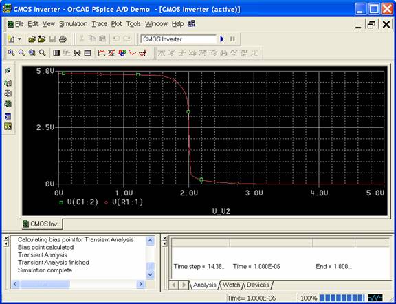
and we have the voltage transfer function for the
inverter.
Let’s look at the rise and
fall times of the circuit. Change the
input voltage source to a VPWL (piece-wise
linear source). Double-click on the
source, and enter the shape of the source voltage:
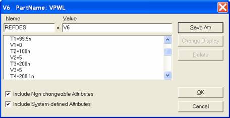
Have the source change from
0 V at 99.9 ns to 5 V at 100 ns, then from 5 V at 200 ns to 0 V at 200.1
ns. This will give a pulse input with a
0.1 ns rise time. Under Analysis – Setup, choose Transient, and simulate the
circuit. In the graph window plot V(R1:1):
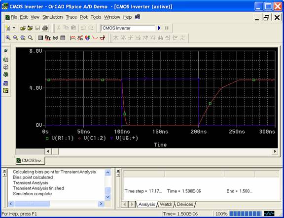
and we can see the rise and fall times of the CMOS
inverter.