


Next: 3 Supplementary Material
Up: Lab 2: Introduction to
Previous: 1 Prelab
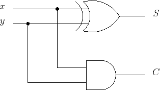
- Write a gate-level Verilog program to implement the half adder circuit.
Figure 1:
Half Adder
 |
- Assign your two inputs to two of the push buttons and your two
outputs to two of the LEDs. Before you continue, ask the
TA to check your assignment.
- Simulate your designed circuit, perform both functional and
timing simulations. Print your waveforms. Are the two waveforms the
same? Discuss.
- Write a Verilog program to implement the same half adder circuit
using dataflow modeling and resimulate your cicuit. Note: you
don't have to respecify your waveforms as you have already saved
them in a file.
- Program your CPLD to implement your circuit and verify that it
works. Ask the TA to initial your labbook once you have it
working.
- Use vectors to describe your inputs and outputs. Send signals to
all of the LEDs to have them off when you send them a logic 0 and
turn on when you send them a logic 1, and similarly, the input to
be logic 1 into your cicuit when to press the button and zero
otherwise.
Next: 3 Supplementary Material
Up: Lab 2: Introduction to
Previous: 1 Prelab
Copyright © 2008, Electrical Engineering Department, New Mexico Tech
Last Modified 2008-09-16