


Next: 2 Lab
Up: Lab 6: Debouncing Switches
Previous: Lab 6: Debouncing Switches
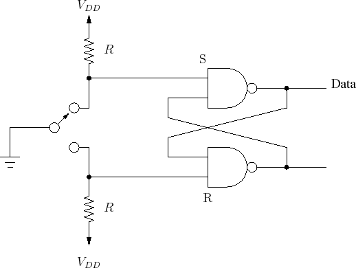
The wavefrom shown in Figure 1 shows the values on S and R when
the switch of Figure 2 is moved from the UP position to the
Down position, then moved back to the UP position. Complete the timing diagram
to show what will be the Data (output of top NAND gate) and Data2 (output of
bottom NAND gate) outputs.
Figure 1:
RS values for above example
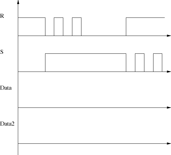 |
Figure 2:
A simple
switch
 |
Copyright © 2008, Electrical Engineering Department, New Mexico Tech
Last Modified 2008-10-10