Next: 3 Supplementary Material
Up: Lab 3: Decoders and
Previous: 1 Prelab
- Place a block of 8 DIP switches on your breadboard, see
Figure 3.
- Connect each lead on one side to VCC.
- Put a 1k resistor from each of the leads on the other side to
ground. Also on this side, place a row of 8 pin headers so that you
have outputs from all of these switches.
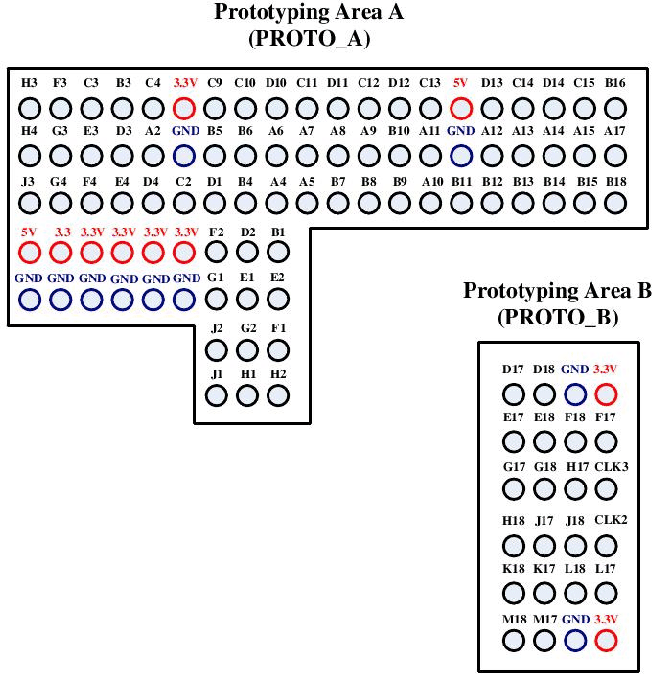
- Use Figure 6 for the pin labels.
- Now that you have all the hardware setup. Design the
BCD-to-seven-segment decoder and test it using different inputs using
the dip switches.
- Implement your multiplexer program that you developed in the
prelab.
Figure 4:
MAX II micro board
|
|
Figure 5:
MAX II micro board with pin headers
|
|
Figure 6:
I/O map of prototyping areas
|
|
Copyright © 2008, Electrical Engineering Department, New Mexico Tech
Last Modified 2009-09-22
![\includegraphics[width=2.5in]{dip_switches.eps}](img5.png)
![\includegraphics[width=5in]{pin_header.eps}](img7.png)