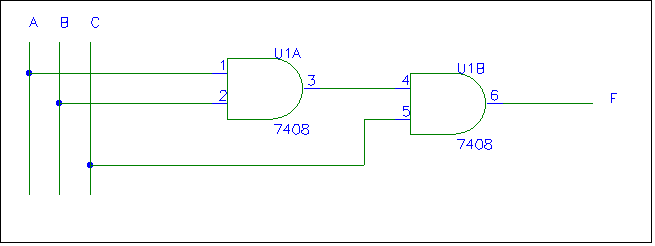
a. From the schematic, derive the Boolean equation for the output, F.
b. Write out a truth table based on the equation you derived in part 3a.
c. Construct the circuit in Figure 3. (Remember to hookup Vcc (+5V) and ground.)
Using a logic probe, observe the values of the output for every possible combination of
input. Construct a truth table with your results.
d. The truth table you derived in part 3b should have agreed with the truth
table you observed in part 3c. If your two truth tables did not agree, list any problems
you found and what you did to correct them.
Questions:
1. Is it possible to create a NAND gate by attaching another gate to the output of
an AND gate? If so, draw a schematic showing how it would be done.
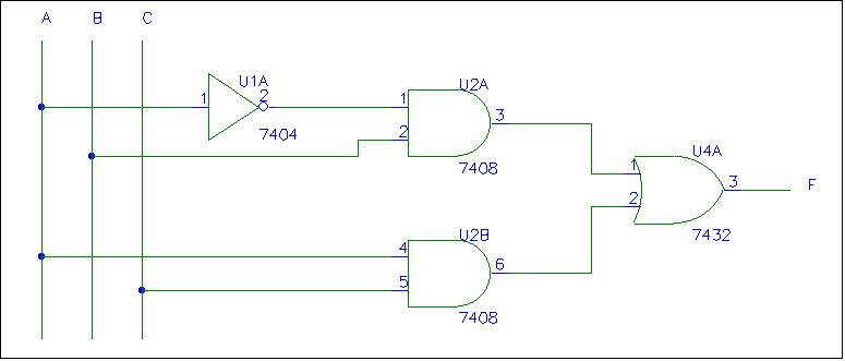
2. Draw a schematic for this Boolean equation: F = A’BC + ABC’ +
ABC. Include chip reference numbers (UX), pin numbers, and gate identifiers (74HCXX)
along with the inputs and output.
3. Draw a truth table for the equation in question 2.