|
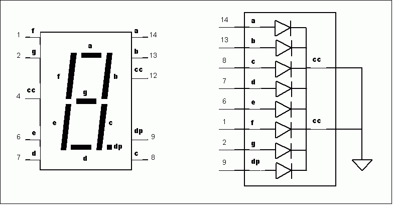
Pre-Lab Exercise 11 Complete the truth table for the MAN74 seven-segment LED that was started in class. (end of pre-lab) EE 101 Lab Exercise 11: 4-Bit Counter/Decoder/Display This purpose of this lab exercise is to familiarize you with the Max+plus II programming environments ability to link two or more design files together for the purpose of completing a single design. You will create a circuit which will integrate a 4 bit counter (from a graphics design file) with a decoder (text design file) to control a MAN74 7-segment LED display. You will demonstrate the MAN74 resetting and display a count from 0 to F, and F to 0.
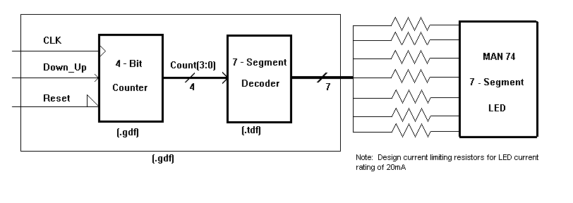
Figure 1: Block Diagram for 0 to F Counter/Decoder/Display Part I In this part of the lab, you will create a graphics design file for a 4-bit counter. 1. Create a separate directory for this lab. Be sure to save all your work from this lab into this directory. Load the Max+plus II software and specify the project name. Use "counter" for the project name in Part I of this lab. 2. Create the graphics design file which will define the 4-bit counter. Altera provides primitives and macrofunctions that you can use in your design file. First, create a new file by choosing New from the File menu. Select Graphic Editor File (with a .gdf extension) and OK. An untitled Graphic Editor window opens. You might want to enlarge this window. Now is a good time to name this file, so choose Save As and name the file. Note: The file name and project name must have the same prefix. In this case, the file name should be counter.gdf. a. To enter a graphics symbol (macrofunction), in this case a 4-bit counter, double click the mouse in a blank space (where you click will determine the insertion point of the symbol, read on). The Enter Symbol dialog box is displayed. Type 4COUNT in the Symbol Name box. Choose OK. The 4COUNT symbol is entered with its upper left corner at the insertion point. Notice the number located in the bottom left corner of the symbol. This symbol ID logs the order in which a symbol is entered on your schematic. Also, note that the symbol is outlined in red. This indicates that it is presently selected. Deselect it by clicking the mouse outside of the selected symbol. For increased readability, you can align symbols to horizontal and vertical guidelines. You can specify the guideline spacing and display or hide the guidelines. Do the following to set the spacing to a 15 by 15 unit grid size, and to show these guidelines: i. Choose Guideline Spacing from the Options menu. The Guideline Spacing dialog box is displayed.b. You may want to move the symbol to another location. To move and align a symbol: i. Click the mouse on 4COUNT to select it.c. Now you are ready to create your input and output pins. The counter you are working with requires these signals to be attached to it: clock, count direction (down or up) and the 4-bit output. There are other pins located on this counter, but for this lab we will not require them. To enter the required signals on your schematic: i. Double-click the mouse in an empty space to the left of the 4COUNT symbol to display the Enter Symbol dialog box. Type INPUT in the Symbol Name box, and choose OK. A generic INPUT symbol is displayed.d. Name the pins. i. Point to the default pin name "PIN NAME" of one of the input symbols and double click the right mouse button. "PIN NAME" will become highlighted. Type "Clock" as a replacement for "PIN NAME".Note: If rubberbanding is turned on (OPTIONS menu), you can move any lines or symbols and still maintain signal connectivity. 3. Compile your program. Remember to save your program and to select the proper device before proceeding with the compilation process. Close the compiler window when a successful compilation is achieved. 4. The .gdf file you have just created will be incorporated into another file. In order to do this, you will have to create a Symbol File (.sym) that represents this file. The symbol you create can be used like any other macrofunction symbol in a Graphic Design File that is at a higher level in the project hierarchy. Create this symbol by choosing Create Default Symbol from the File menu. For some types of design files, a symbol may have been created when you first saved the file. If so, you will get a message asking whether it is OK to overwrite the existing symbol. Choose OK to ensure that you have the most up-to-date information in your Symbol File. Choose Close from the File menu or double-click the mouse on the Document Control Menu box. The Graphic Editor window onto the .gdf file you just created automatically closes. 5. Simulate your program (File - New - Waveform (.scf)). Set an End Time of 8.0us and a grid size of 100ns. When you are ready to list your input and output signals, check only the input and group boxes. If you check the output box, you will place four separate count lines in your simulation file. The group signal for these will be much easier to read. Make these modifications to your input signals (Highlight part of signal to be modified, Edit - Overwrite): Reset should be high until the 7.0us mark, low thereafter. Down_Up should be high until the 3.5us mark, low thereafter. Clock should continue from 0us to the end of the simulation. Zoom out so that you can see the entire simulation in a window. Verify that the counter is working correctly. Change the print setup to landscape and print the simulation. You will have to fold the printout for it to fit in your lab notebook. Print out a copy of your .gdf file and paste it in your
notebook.
Questions for Part I: 1. When setting up your simulation file, how does specifying "groups" instead of "outputs" affect the data provided by the simulation? 2. Describe how the reset signal affects the output of your counter. 3. Describe what happens when the Down_Up signal
is toggled.
Part II At this point, you should not have any files open on the
Altera desktop. Create a .tdf file to define the truth table for a hexadecimal
to seven segment LED decoder. Name this file "decoder.tdf" and establish
the Project Name as "decoder." When first saving this file, MAKE SURE
YOU SAVE TO THE SAME DIRECTORY THAT YOU USED IN PART I ! Follow the
pattern in Figure 2 when creating this file. The beginning and end of the
file have been provided for you.
SUBDESIGN decoder (
BEGIN TABLEEND;Count3, Count2, Count1, Count0 => a, b, c, d, e, f, g;END TABLE; Figure 2: AHDL .tdf File for Seven Segment Decoder Be sure to name your four inputs the same as you named the outputs from the counter file you created in Part I. If you dont, your files will not be able to "talk to each other" later. When you are finished with your decoder, save and compile as usual. Create a symbol file for this decoder like you did for the counter in Part I. Simulate your decoder and verify that the outputs agree with the truth table you created for the pre-lab. Print out a copies of your .tdf and simulation files and paste them in your notebook. Again, you will probably have to do some folding. Have a lab assistant verify your results before proceeding. Question for Part II: 4. What is the obvious advantage for using a truth
table format as opposed to Boolean equations for every output when designing
an AHDL file to decode binary numbers to a 7 segment display?
Part III
You will now create a .gdf file to link your two previous files together. Again, make sure you are working in the proper directory. This file will be referred to as the Top Level GDF. Before starting, change your project to "lab11". Create a new .gdf file and name it "lab11.gdf". You will now grab the other two files (symbol files) you created in Parts I and II and incorporate them into this file. Do this by selecting Symbol and Enter Symbol from the menu bar. Then type in (or select from the list) the symbol files you created. This will bring up a symbol for each file, and you can place these where ever is convenient on the desktop. You will need to insert and label input and output symbols for any pins that are physically on the EPLD (as you did in Part I). The inputs to the EPLD will be the clock, reset, and down/up signals. The outputs will be the 7 control lines that will attach the EPLD to the 7 segment decoder. Internal signals, such as Count0, Count1, Count2, Count3, and the bus Count(3..0) do not need symbols attached, but their wires must be drawn (extended) and they must be properly named. The internal lines do not have to be physically attached, since the software will recognize connectivity through the similar names (like you did in the 4-bit counter file). Once you are done with this gdf, save and compile it. Load up the report file for this part of the lab, add your name to it, and print out a selected area that includes the chip pin assignments. This is most of your schematic for your circuit. From the Max+plus II menu, select Hierarchy
Display. This will show you how your files are integrated together
to form one project.
Question for Part III: 5. List some advantages of creating and simulating
a design project in separate parts (like the first two parts in this lab)
instead of all in one design file.
Part IV Create a simulation file that covers the entire project. Name it the same name as your overall project (i.e. - lab11.scf). Set the file size and grid spacing so that 40 complete clock cycles can be observed. When choosing these parameters, consider the following: The input signals you should be concerned with are the clocking, reset, and up/down signals. (Do not select the other input options, if any are given). Refer to Part I for help in selecting the input signals you wish to display, and how to configure each one (i.e. - Down_Up should be high until 3.5us, low elsewhere, etc.). The only output signals you are concerned with are the outputs from the decoder truth table. Run the simulation file, and take note of a few input/output relationships to check for accuracy. You dont have to check every single one! Fold the simulation and paste it in your lab book. After you are satisfied that this simulation is correct,
print out a copy of your top level .gdf file and paste it in your notebook.
Question for Part IV: 6. Why am I making you simulate (and verify) each
part of this project before you proceed to the next part?
Part V Program an Altera EPM7032LC44-15 PLD with your lab11.pof
file. Build the circuit. Connect the clock input to the TTL signal on your
protoboard, the Down_Up input to one debounced switch (normally high) and
the Reset input to the other debounced switch (normally high). Connect
the seven outputs through current limiting resistors to the appropriate
inputs on the MAN74. The LEDs that make up the MAN74 are designed to operate
at 20 mA. As such, choose any resistor values between 250W
and 1KW to current limit each LED.
|