|
Note: The procedures outlined in this lab are outdated for EE101. PSPICE Artwork generation is now utilized instead of the hand-drawn method given here. Still, the rest of the information given in this lab is of value. (There is no pre-lab exercise for this lab. Rather, the pre-lab is all of the preparation done in prior labs to get to this point of the project. Also, no lab-writeup is required for this lab - other than the formal report.)
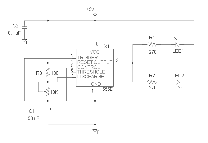
The use of printed circuit boards (PCB) are desired over breadboards and other circuit building techniques whenever a permanent circuit is needed. Signals generated in a circuit constructed on a PCB are generally cleaner than those coming from temporary circuits. Also, PCBs can hold up under a lot more stress. The purpose of this lab is to introduce you to one method of building a PCB. You will build a circuit around a 555 timer chip that will alternately light two LEDs. The rate of the flashing will be adjustable through a 10KW potentiometer. The schematic for this circuit is in Figure 1.
Figure 1: 555 Timer Circuit Theory of Operation For the circuit configuration in Figure 1, the frequency of oscillation (measured from pin 3) is determined from the following formula:
Using the component values given in the circuit, when Rpot is
set for 0W , the rate of oscillation is 9.6
Hz. Adjusting Rpot for its maximum value of 10KW
, the oscillation rate reduces to only 0.46 Hz.
Light emitting diodes (LED) will glow when they are conducting current. If the potential is greater at the cathode of an LED than at the anode (represented by the flat line at the point of the triangle), current will be conducted. Hence, when the oscillating signal from pin 3 is low, LED1 will conduct electricity and light up. If the signal from pin 3 is high, LED2 will light glow. LEDs used in this circuit are rated to operate with a current of 20mA. Any current greater than this could stress each LED (and probably burn it out). The oscillating signal from pin 3 has an amplitude of 5V. To limit the LED current to 20mA, a current limiting resistor should be placed between each LED and pin 3. The value of this resistor is determined by Ohms Law, as follows:
We select a value of 270W for the resistors. This is primarily due to the availability of that value in the normal lab stock. For "overdesign" considerations, we may wish to try 1000W resistors instead. The selection of this larger resistor value is in the interest of conserving current through the LEDs. The 0.1m F capacitor, C2, acts as a filter
for the 5V power supply.
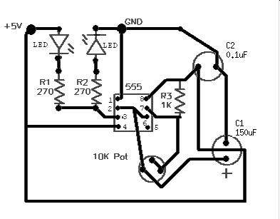
Board Layout A view of how the components will fit together on the printed circuit
board is shown in Figure 2.
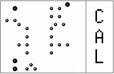
Figure 2: Component Layout - Top View Figure 3, 4, and 5 represent various stages of what your printed circuit
board will look like before you actually etch it. Figure 3 shows the location
of the pads for each component. Figure 4 shows the connections,
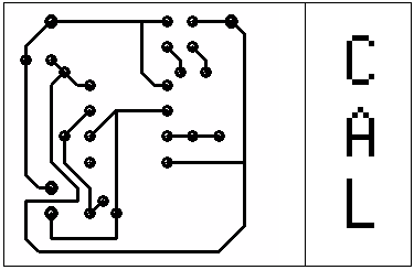
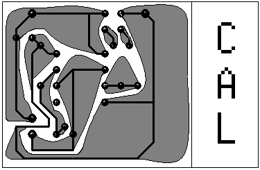
or traces, between each pad, and Figure 5 shows the board after
you have planned for copper maximization. Note that Figures 3, 4,
and 5 are the mirror image of the component placement in Figure 2. This
is because you will be soldering to the bottom of the board while the components
will be on the top.
Figure 3: Location of Component Pads
Figure 4: Traces Connecting Components
Figure 5: Copper Maximization
Procedure (The order may be switched on some steps) 1. Obtain a single sided copper board from the lab instructor. Use steel wool to shine the copper side of the board. Wash the board with soap and dry using a clean, lint free cloth. Take care not to leave any finger prints on your board. 2. Using dry transfers, apply the proper pads to the copper board, as shown in Figure 3. Take care to use the proper spacing, and be sure to leave 3/4" to the right of your board for your initials. You may wish to make a copy of Figure 3 and use the copy as a pattern for your pad spacing. Using an etch resistant pen (Sharpie or other), mark your initials on the board. 3. With the help of a lab TA, drill the center holes out of the pads. 4. Using an etch resistant pen, draw in the basic connections between the components as indicated in Figure 4. 5. Using an etch resistant pen, thicken the traces to maximize the copper left on the board, as shown in Figure 5. 6. Etch your board. When it is finished etching, rinse and dry it. Then, rub the board gently with steel wool until the ink and dry transfers are removed, revealing the copper pads and traces. 7. Solder the components into the board, along with a red wire for the +5V connection and a black wire for the GND connection. 8. Verify that there are no shorts in your board. 9. Demonstrate that your pc board works.
|