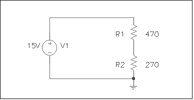
- Label each node in the circuit. (there are three, including ground)
- Determine the Req for the circuit.
- Find the current through the circuit.
- Find the voltage at each node. (that is, the total voltage between that node and gound).
Next, using any methods we have covered to date in class, determine the voltage drops across each resistor and all the indicated currents. Perform a power balance as a means of checking your work. (Big hint - refer to the example given in your class notes last week!)
(end of pre-lab)
Lab Exercise 3: Introduction to PSPICE
In this lab you will learn how to use PSPICE to analyze resistive networks containing a DC voltage source.
Log on to the computer (NT mode). It is a good idea to keep all of your
computer work for this class in a separate directory structure. "ee101"
would be a logical name for the parent directory, and each lab number for
the separate lab exercises. For example, you may wish to keep the work
for this lab in U:\ee101\lab3. If you are not familiar with creating directories
ask someone to assist you.
- Once you are logged in, to call up PSPICE, go down to the taskbar and click on the Start button. Go to the Programs menu and bring up the DesignLab Eval 8 menu and select Schematics.
- You will now enter and analyze the first prelab circuit given again below.
- Before you begin to draw anything, go to the Options menu and select Display Options. Make sure all the options boxes are selected. Then, go to the Analysis menu, select Display Results on Schematic, and make sure "Enable" is not checked. (You will enable this feature later during this lab.)
- With the mouse, choose the Draw menu bar. Under that, select Get New Part. Then click on the Libraries button.
- A parts name window will appear. Below, windows listing the libraries and the parts contained within them appear.
- First, let's place two resistors on the PSPICE desktop. Resistors are located in the analog.slb library. Select this library and select R (for resistor). Select Place & Close.
- An image of a resistor appears on the desktop. Click the left mouse button to place the resistor. Note that a permanent resistor has been added to the desktop, and that you still have a floating image of a resistor. Since you need two resistors for this circuit, go ahead and click the mouse to place the second one also. Click the right mouse button to deselect the resistor (so you don't add any more to your desktop). If you ever add components to your desktop that do not belong there, you can select them with the left mouse button and hit the del key to erase them.
- Rotate your two resistors so they line up with the way the schematic is drawn. Do this by selecting a resistor with the mouse (one at a time, it should turn red) and then going to the Edit menu and choosing Rotate. (The shortcut keys to rotate a selected object are <CNTL-R>). Do this for both resistors. Then, line up the resistors by selecting one and using the mouse to drag it so that it touches the end of the other.
- Now you will add a source component to your schematic. Like before, go to Get New Part. This time, choose the source.slb directory and choose Vsrc. Place this voltage source on the schematic by clicking the left mouse button, and then click the right mouse button so you don't place another source. You need to define the voltage value of this source. Do so by double clicking the left mouse button on the red (selected) component. A window should pop up that has several options for this source. Scroll down to the DC = line, and type 15 (for 15 volts). Save the attribute and click on OK.
- You need to define the resistor values as well. Select each resistor and replace the default resistor values with 470 and 270. To make your schematic more readable, you may wish to select the text around the resistors and move it to the side slightly.
- Now connect your components together by going to the Draw menu and selecting Wire. Use the mouse to place the wires between all components (left mouse button to start drawing, left to stop, space bar to start again).
- You must now add a ground to your circuit. Find AGND in the port.slb directory, and place it where indicated on your schematic. PSPICE simulations will not work unless you have defined a ground reference for your circuit.
- Perform an electrical rules check to be sure your circuit schematic will simulate properly. (Analysis menu, Electrical Rule Check).If all goes well, you will see a small window flash on the screen and nothing else). If no errors are reported in your schematic, proceed to the next step. If errors are reported, fix them now. If you have not done so, now is a good time to save your schematic. Choose a name that will help you identify which problem this is. Ask for help if you need it.
- Now you will simulate your circuit. Do this by going to the Analysis menu and choosing Simulate. When the circuit is finished simulating, a PSPICE window will appear. Select File in this window, and Examine Output. Scroll down towards the bottom of the file until you come to a series of headings that say Node and Voltage. The voltage at each circuit node should be reported. Identify which node voltages are associated with which circuit elements and note this in your lab book.
- Scroll further down the output file. Note the source current and total power dissipation for the circuit are reported. The voltage source current is reported as -2.027E-2, or -20.27 mA. You have already calculated Is for this circuit in the pre-lab. Does your answer agree with PSPICE's?
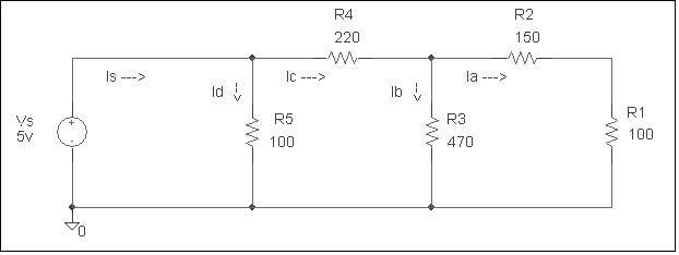
- Enter the circuit from Exercise 2 of the pre-lab in PSPICE and simulate the circuit. With the information provided by the PSPICE simulation (node voltages and the source current), use KVL, KCL, and Ohm's Law to determine all the voltages and currents associated with the circuit. Show all your work in your lab write-up.
- After you have completed all your calculations in the previous step, verify that your answers are correct by comparing them to the lab instructor's key or to your prelab. Fix any mistakes you have.
- Go to the Analysis menu, select Display Results on Schematic, and check the Enable command. Now look at your schematic!
Here is how you would draw this schematic in PSPICE:
Note: If you attempt to select a part and it and a box appears
around it, and it does not turn red, then you have not selected the
object, but the text around it. This is fine for moving text, but
for moving the component, you must align the mouse on the part itself and
click the left mouse button. If you select text by accident,
click the right mouse button to deselect it. Then, try to select
the component.
- What are the advantages of using PSPICE to analyze a circuit? What are the disadvantages?
January 2001
Copyright 2001, New Mexico Tech