EE101
Pre-Lab Exercise 6
THIS PRE-LAB EXERCISE WILL BE COMPLETED AS A CLASS, THE DAY
OF THE LAB!
Using the general layout in Figure 1, design a circuit, which will produce
a TTL compatible signal. You are to design a circuit so that the signal,
output at X1-3, will have a frequency range from about 1Hz to 10Hz. This
signal will drive two LED's which will alternately flash. Your business
manager has told you that your company has an over-abundance of 10 Kohm
potentiometers and 150uF capacitors. Therefore, select Rvar and C1 so that
you can make use of one of these. When designing your circuit for R1, R2,
R3, LED1, and LED2, take note that:
-
The LED's have a nominal current rating of 5mA.
-
An acceptable design is one in which the lower and upper frequency limits
are within 10% of the specified values.
-
Specific resistor values between 1 Kohm and 1Mohm are available.
-
The TTL output signal has a frequency equal to f = 1.44/((R1 + 2R4)(C1))
hertz.
Once you have designed your circuit, perform separate calculations for
Rvar = 1Kohm, 3Kohm, 6Kohm, and 10Kohm.
Your pre-lab should include a completed schematic with all circuit element
values along with the math you used to design all aspects of your circuit.
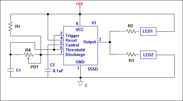
Figure 1
EE 101
Lab Exercise 6: The 555 Timer
In this lab exercise you will complete the first stage of your EE101 semester
project. Later in the semester you will need the setup information and
results from today's lab. Therefore, it is important that you keep all
of this today's work in a safe, easy to find location. It is highly recommended
that you create a separate subdirectory for this and all remaining labs.
You may also wish to backup this work on a floppy disk when you have the
chance.
For this lab, you will use PSPICE to simulate your design, and
to verify that your design is a valid one.
Part I - Entering your schematic in PSPICE
-
Using the PSPICE schematic capture program, enter the schematic that you
designed in the pre-lab. Refer to Figure 1 to help you with parts placement
and attributes. Parts of the schematic in Figure 1 are deliberately left
out. These items are left for the student to put in. (The 555 timer and
diodes are located in the eval library and the potentiometer is located
in the breakout library).
Below are some items to help you define certain elements of your
circuit:
-
The part name for the variable resistor is POT. Under attributes, define
its package type as a TO-39 and its value as {Rvar}. (The brackets around
this name allow for you to designate the potentiometer's value as a changeable
parameter).
-
LED's are not defined PSPICE's libraries. For these parts, use the diode
D1N4148. Rename the D1 and D2 designators LED1 and LED2. Make sure you
orient them correctly in your schematic.
-
To simulate the potentiometer, you will use a feature in PSPICE named "parameters".
To set this up, first add the part "PARAM" (located in the special library)
to your schematic. Place the parameters block to the side of your schematic.
Edit the parameters attributes as follows:
Name1 = Rvar
Value1 = 0
-
Under the Analysis menu, choose setup and configure the following:
Bias Point Detail - make sure this is selected
Parametric - Swept Variable Type = Global Parameter
Sweep Type = linear
Name = Rvar
Start Value = 1K
End Value = 10K
Increment = 1K
Transient - Print Step = 0.1s
Final time = 3s
-
Be sure to hook up power (+ 5VDC), ground, and a voltage marker to your
circuit (the +5 volt reference shown in Figure 1 is not a true power source).
Part II - Simulating Your Design
-
Perform an electrical rule check on your circuit. If this reports any errors,
fix them at this time.
-
Simulate your design. After several seconds of calculations, the Probe
window will pop up with a smaller window in front of it. In this smaller
window are the ten settings for Rvar. All are selected at first. Deselect
all of them by clicking on "None." Then, select the Rvar = 1K setting with
your mouse and click on "OK." A waveform will appear. Using the cursors,
measure the period of this waveform and calculate its frequency. Verify
that this frequency is close to what you calculated it should be in the
pre-lab. Print out a copy of the waveform.
-
To check how your circuit reacts with different values of Rvar, simply
go back to the schematic and re-simulate (just hit the F11 key). Then,
when the probe window comes up, select the value of Rvar that you want
to observe the waveform for. Do this for Rvar = 3Kohm, 6Kohm, and 10Kohm.
Compare these results to those you calculated in the pre-lab and print
out the waveforms for each.
February 2001
Copyright 2001, New Mexico Tech