Prelab Exercise 8
Given the following Boolean Equation:
F = ABCD + A!BC + AB!C + A!B!CD (Note:
A!BC reads "A, not B, C")
-
Draw and fully label a schematic using only 04's (NOT's), 08's (AND's),
and 32's (OR's).
-
Using a KMAP, derive the minimum equation for the original formula.
-
Draw and fully label a schematic from the reduced equation using only 04's,
08's, and 32's.
Lab Exercise 8: Introduction to Logic Gates
The pinout schemes for the logic gates you will be using in this exercise
are
given in Figure 1. Note that for all of these chips, Vcc = 5V (pin 14)
and GND = 0V (pin 7). Also, note that the pins that are inputs on some
chips are not necessarily the inputs on other chips!
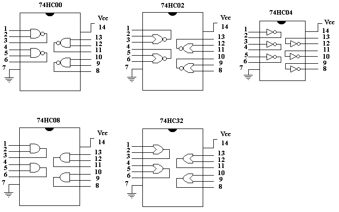 Figure 1
-
Fill out the truth tables for three gates above (specifically, the NOT,
AND, and OR gates). Under V indicate the voltage of the output,
as indicated by a voltage meter. Under F, record the logic
level ("1"or "0") as indicated by the logic probe.
| 74HC04 (NOT) |
74HC08 (AND) |
74HC32 (OR) |
| A V F |
A B V F |
A B V F |
| 0 |
0 0 |
0 0 |
| 1 |
0 1 |
0 1 |
|
1 0 |
1 0 |
|
1 1 |
1 1 |
-
The following exercises deal with the schematic in Figure 2.
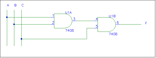
Figure 2
-
From the schematic, derive the Boolean equation for the output, F.
-
Write out a truth table based on the equation you derived in part 2a.
-
Construct the circuit in Figure 2. (Remember to hookup Vcc (+5V) and ground.)
Using a logic probe, observe the values of the output for every possible
combination of input. Construct a truth table with your results.
-
The truth table you derived in part 2b should have agreed with the truth
table you observed in part 2c. If your two truth tables did not agree,
list any problems you found and what you did to correct them.
-
The following exercises deal with the boolean equation in the prelab:
F = ABCD + A!BC + AB!C + A!B!CD
-
Construct a truth table based on this Boolean equation.
-
Build this minimized circuit. For every high and low combination of the
inputs, test your circuit by using a logic probe. Construct a truth table
showing your results. This truth table should agree with the truth table
you derived from the unsimplified circuit (from part 3a). If they do not
agree, find out where the problem is before proceeding. Don't disassemble
your circuit until you have demonstrated that it works to a TA.
Questions:
-
Draw a schematic for this Boolean equation: F = A'BC + ABC' + ABC. Include
chip reference numbers (UX), pin numbers, and gate identifiers (74HCXX)
along with the inputs and output.
-
Draw a truth table for the equation in question 1.
-
How many gates (and, or and not) did your circuit require in Part 1 of
the pre-lab? In Part 3?
March 2001
Copyright 2001, New Mexico Tech