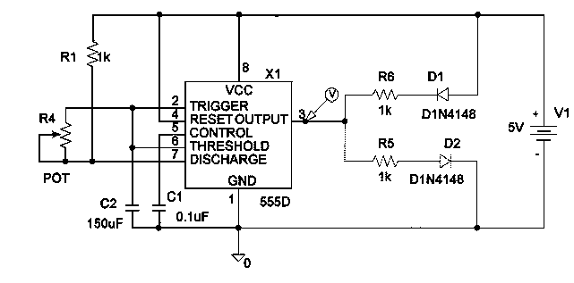
Figure 1
In Phase I of the class project (lab 6), you designed and simulated a circuit that would alternately flash two LED's while outputting a TTL compatible waveform adjustable from about 1Hz to 10Hz. In Phase II (lab 7) you prototyped your design on a breadboard and enhanced it to provide outputs over a much wider frequency range. In Phase III, you will scale back your design to the original specifications from lab 6. Your design should be similar to the one in Figure 1.
Figure 1
Execute the MSIM Schematics program. Open your design file from Lab 6, and save it under a new name (Click File - Save As) in your account.
Take a few minutes to verify that each circuit element (R's, C's, diodes, the potentiometer, and the 555) has a package type defined for it.
From the Tools menu, select Run PCBoards. The Microsim PCBoards program will start and the netlist from your design will be loaded (see Figure 2). There may be some warnings or errors reported with your netlist. Warnings are generally okay, but if you get any errors you will have to give them attention before proceeding.
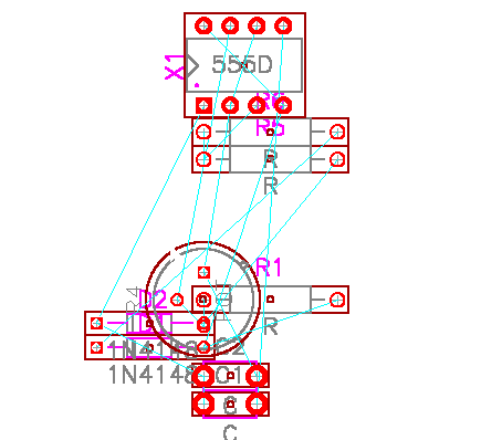
Figure 2
Figure 2 shows a jumbled mess of your components and their "footprints" (package types). The light lines connecting all of these are called the "rats nest." You will be responsible for placing these footprints in such a way that they can be connected together easily. First you will draw a component "keep in" border. The Board Signal Keepin is a rectangle, shown in Figure 3, which will define the size of your printed circuit board. To draw this go to the Draw menu and select Board Signal Keepin. The grid spacing on the desktop is measured in mills, with the default being that each dot is 50 mills apart. At the lower right on the screen are two numbers reported in mills, which report the cursor position on the screen. Make the rectangle 2.0" wide (2000 mills) and 1.9" (1900 mills) high around the components and rats nest, as shown in Figure 3.
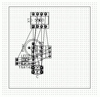
Figure 3
Next you will move each component to a proper position within the keepin layer. Use Figure 4 as a guide. Move each part by selecting it with a mouse click and dragging it to its proper place. Rotate parts (Ctrl+R) as you need to, but do not flip sides or mirror any footprints. This could result in your artwork not matching your schematic.
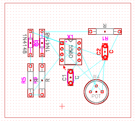
Figure 4
Click on the board layer field box on the toolbar (it probably is set for "Component") and change the board layer to "Solder".
The first editing you need to do is select each component pad (the place where the component leads go through the board) by double clicking on the center of the pad. This should bring up an attributes window for the selected pad. Select PIN_PADSTACK and set the value to (rnd or sq)-080-040. This will size all of the pads so that their outer diameter is 80 mils and they will all have a 40 mil hole in the center.
Next, following the connections in the rat's nest, you will draw the actual connections, or traces, of your design.
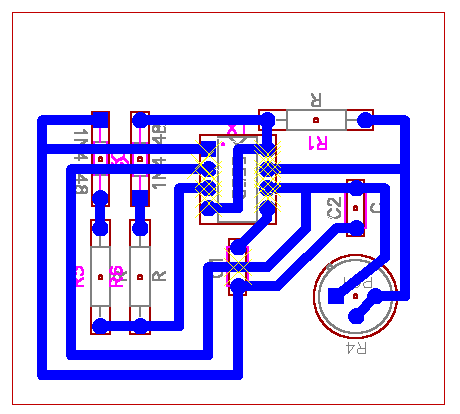
Figure 5
Now you need to add a couple of places on your board to attach your VCC (+5V) and ground inputs. As shown in Figure 6, draw traces up to the location where the VCC and ground pads are shown (make sure to do this on the solder layer). Then, add the pads (Draw - Component - Jump1). An "X" will appear where you have added your new connections. This indicates that the two traces touching at that point do not have the same name. Normally, this would be a cause for concern, but not at this time. Ignore the "X's". Finally, add text blocks for VCC and GND and mirror them, as shown in the figure.
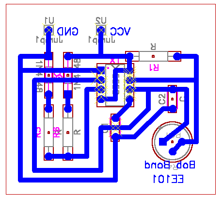
Figure 6
In order to have your artwork print out properly, your entire design needs to be moved to a specific area on the desktop. Select your entire design by lassoing it with the mouse. Move the selected area so that the lower left-hand corner of the block is at grid location 2400, 3700. This way, your design should print out near the center of the page. At other locations, it may not print out at all.
__________________________________________________________________________________
The rest of this experiment will be during the etching session that each of you must schedule!
Printing Instructions (to be done prior to etching, and with supervision).
Printing your artwork to "blue paper" can be one of the trickiest parts of circuit board construction. First of all, you should use a printer that does not get a lot of traffic; otherwise, you may end up etching somebody's term paper.
Once you have a paper copy of your artwork, cut a piece of blue paper to cover the image and tape it, dull side up, over the image on the paper. Use only a little tape at each corner. Run the original print with blue paper through the manual feed of the same printer you first printed out to, and reprint.
Ironing, etching, and stuffing your board will be covered by demonstration.
Copyright 2002, New Mexico Tech