EE 231
Lab 4: Design of a 4-Bit Adder using 1-Bit Full Adder Blocks

Prelab 4

In this lab you will design a 4-bit adder using a 1-bit full adder as a building block as shown in Figure 5.6, page 227 of Brown. You will first complete the design of the 1-bit full adder in Altera, then use the Altera graphical editor to combine four 1-bit full adders into a 4-bit adder. Rember to do each week's lab in a seperate folder, today's lab should be in U:\EE231\lab4\!!

  1. Design a 1-bit full adder in Altera using one of the following methods. There are several ways to implement designs in Altera. Shown below are four implementations of a full adder using Altera Text Design Files (TDF), a fifth method using a Waveform Design File (WDF), and a sixth possibility using an Altera Graphic Design File ( GDF).
    1. A TDF using a factored form of the Boolean logic shown in Figure 5.4(b), page 225 of Brown (cout=ci+1):
             SUBDESIGN fulladdr
                  (
                      a,b,cin     : INPUT;
                      sum,cout    : OUTPUT;
                  )
                  BEGIN
                      sum = (a $ b) $ cin;
                      cout = ((a # b) & cin) # (a & b);
                  END;
      
    2. A TDF using if-then structure:
             SUBDESIGN fulladr
                  (
                      a,b,cin     : INPUT;
                      sum,cout    : OUTPUT;
                  )
                  BEGIN
                      if    (((0,cin)+(0,b)+(0,a)) ==0) then
                          (cout,sum) = 0;
                      elsif (((0,cin)+(0,b)+(0,a)) ==1) then 
                          (cout,sum) = 1;
                      elsif (((0,cin)+(0,b)+(0,a)) ==2) then
                          (cout,sum) = 2;
                      elsif (((0,cin)+(0,b)+(0,a)) ==3) then
                          (cout,sum) = 3;
                      end if;
                  END;
      
    3. A TDF using arithmetic operations:
             SUBDESIGN fulladr
                  (
                      a,b,cin     : INPUT;
                      sum,cout    : OUTPUT;
                  )
                  BEGIN
                      (cout,sum) = (0,cin)+(0,b)+(0,a);
                  END;
      
    4. A TDF using a truth table Figure 5.4(a), page 225 of Brown:
             SUBDESIGN fulladr
                  (
                      a,b,cin     : INPUT;
                      sum,cout    : OUTPUT;
                  )
                  BEGIN
                      TABLE
                      cin,   b,   a  =>  cout,  sum;
                        0,   0,   0  =>    0,    0;
                        0,   0,   1  =>    0,    1;
                        0,   1,   0  =>    0,    1;
                        0,   1,   1  =>    1,    0;
                        1,   0,   0  =>    0,    1;
                        1,   0,   1  =>    1,    0;
                        1,   1,   0  =>    1,    0;
                        1,   1,   1  =>    1,    1;
                      END TABLE;
                  END;
      
    5. You could also enter the design as a waveform using the Altera Waveform Editor to enter a Waveform Design File

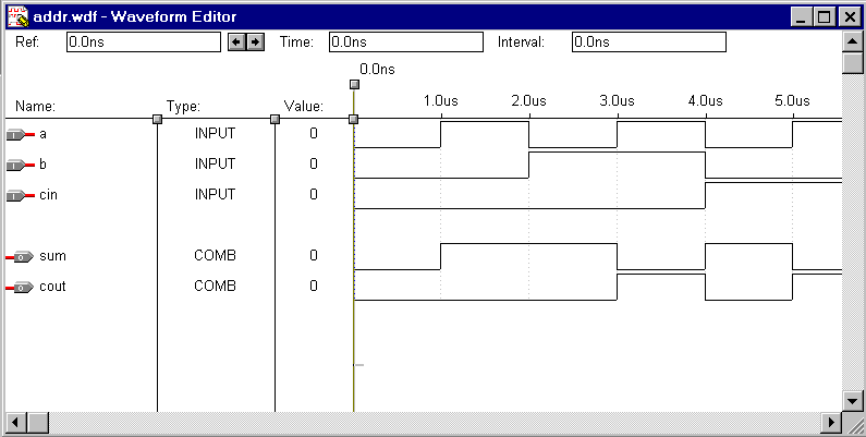
      (See Altera Max+Plus II Getting Started online help to see how to do this.)

    6. Another way would be to use the Graphical Editor to enter the gate representation shown in Figure 5.4(c), page 225 of Brown, in a Graphic Design File (GDF). (Details on using the Graphical Editor are discussed below.)
  2. After entering, compiling and simulating the full adder, switch back to the text editor window (if you used a TDF) containing your design. Choose Create Default Symbol from the File menu, and choose OK to create the fulladdr.sym Symbol File. This fulladdr.sym can be imported into a Graphical Design File as a building block for larger circuits.  Close all open windows within the Max+II main window.
  3. Design your 4-bit adder using the Altera Graphical Editor. Start a new project from the Project Name submenu of the File menu, give it the name 4bitaddr. Go to File, New, and open a .gdf file. Go to File, Save As, and save the .gdf file with the project name -- i.e., U:\EE231\lab4\4bitaddr.gdf.

    In an open area of the Graphical Editor, double-click with the left mouse button. In the Enter Symbol dialog box, enter the name of your 1-bit full adder (fulladdr.sym). Repeat this until you have four full adders displayed vertically.

    In the empty space to the left of the full adders double-click the left mouse button. In the Enter Symbol dialog box, enter INPUT in the Symbol Name box, and choose OK. The INPUT symbol is then displayed.

    Press left mouse button to select the INPUT symbol then use the right mouse button to create a copy (then paste) of the symbol and place it below the original. Repeat until you have eight inputs.

    Repeat the above steps to create five outputs using the OUTPUT symbol.

    Point to one of the input pins and double-click the left mouse button. Type the name you wish to give this input (e.g., A0. Repeat until all eight inputs (A0-A3 and B0-B3) are named. Do the same for the five outputs (S0-S3 and Cout).

    The Cin input to the first 1-bit adder needs to be connected to GND. Double-click the left mouse button near the Cin input of the first adder and choose the symbol GND.

    Connect the input symbols to the inputs of the full adders, and the outputs from the full adders to the output symbols. Also cascade the cout from one full adder to the cin on the next. Connect the cout from the last full adder to the COUT output symbol. To make connections, point one end of the connection, press and hold down the left mouse button, drag the mouse to the other end of the connection, and release the mouse button.

  4. After the drawing is complete, save the .gdf file. Open the Compiler window, and compile your design. If the compiler finds any errors, correct them.
  5. Create an .scf file to simulate your design. Enter all possible input values, and make sure the outputs are correct. Print a portion of your waveform. HINT: You may want to learn how to group signals!!
  6. Program your 4-bit adder into a 7064 chip. (Don't forget to choose the device EPM7064LC44-15)
  7. Use the logic analyzer and stimulus generator as you did last week to verify that your design works. For the stimulus generator, as you have done previously, used the 74HC4040A counter chip (how many of the Qi's will you need?).


September 2000
Copyright © 2000, New Mexico Tech