CS_MEM_EVEN
and CS_MEM_ODD lines to the logic analyzer. Do not disconnect the
logic analyzer until the end of the lab - you will use it in later parts
of the lab.
ldaa #$aa
staa $2000
ldaa #$55
staa $2001
ldaa $2000
ldab $2001
std  $2002
jmp  $100A
Execute the program. Look at the bus signals on the logic analyzer.
- (a)
- Verify that the time E is high and low match the values from the
Electrical Characteristics manual.
- (b)
- Identify the cycle where the HC12 reads the byte from address
0x2000. Verify that A0, LSTRB, R/W,
CS_MEM_EVEN,CS_MEM_ODD, OE and WE agree with what you expect from Table 13 of the Technical Summary manual. Also verify that the data read from address 0x2000 is on the part of the data bus you expect. How long does it take fromCS_MEM_EVENgoing low until the 0xaa from address 0x2000 is on the data bus? Does this agree with the access time from the memory data sheet? - (c)
- Identify the cycle where the HC12 reads the byte from address 0x2001.
Verify that A0, LSTRB, and R/W,
CS_MEM_EVEN,CS_MEM_ODD, OE and WE agree with what you expect from Table 13 of the Technical Summary manual. Also verify that the data read from address 0x2000 is on the part of the data bus you expect. - (d)
- Identify the cycle where the HC12 writes the word to address 0x2002.
Verify that A0, LSTRB, and R/W,
CS_MEM_EVEN,CS_MEM_ODD, OE and WE agree with what you expect from Table 13 of the Technical Summary manual. Also verify that the data written to address 0x2002 is on the part of the data bus you expect. - (e)
- The HC12 is running an infinite loop which executes the last four
instructions in the simple program above. Identify the cycles where the
HC12 fetches the instruction
ldaa $2000.
- (a)
- Verify with the logic analyzer that the E-clock is not stretched.
- (b)
- Connect your expansion port EA to LEDs on your breadboard. Use
DBug12 to check to see whether expansion port EA still works. You can
test this by making one of the expansion ports an output port, and seeing
if you can turn the LEDs on and off with expansion port EA.
- (c)
- Use DBug12 to check to see whether the memory expansion still works. You
can do this by using the MM instruction to see if you can
successfully change the value of memory in the expanded address space.
- (d)
- Be sure to modify your startup code at address 0x0D00 to add one E-clock
stretch so your expanded memory will continuer to work.
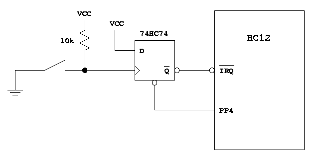
Write a program which enables the IRQ interrupt, and makes it level sensitive. Also, make expansion port EA and output port, and write 0x00 to it. (You should still have EA connected to your LEDs from the previous section of the lab.) In your IRQ interrupt service routine increment EA. Be sure to clear the source of the interrupt in your interrupt service routine.
- (a)
- Verify that your program works. Each time you push your switch you
should see EA increment by one.
- (b)
- Set your logic analyzer to trigger on the falling edge of the IRQ line.
Push the switch to generate an interrupt. Determine the amount of time
it takes from the falling edge of IRQ to the pulse on PP4 which clears
the interrupt flip-flop. Explain why it takes this amount of time.