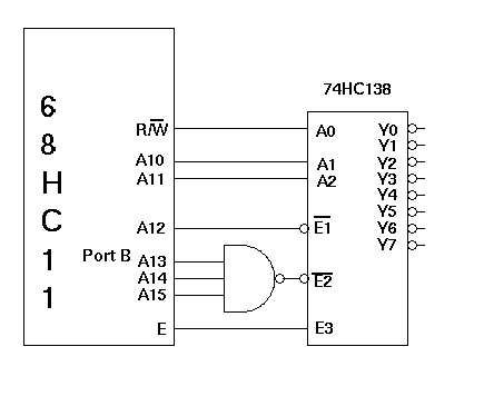
- For what address range will output Y2 be selected? Will it be used as
a chip select for an input or output port?
A15 A14 A13 = 1 1 1 A12 = 0 A11 A10 R/W = 0 1 0 Addr = 1110 01XX XXXX XXXX, R/W = 0 Addr = 0xE400 - 0xE7FF Output - For what address range will output Y5 be selected? Will it be used as
a chip select for an input or output port?
A15 A14 A13 = 1 1 1 A12 = 0 A11 A10 R/W = 1 0 1 Addr = 1110 10XX XXXX XXXX, R/W = 1 Addr = 0xE800 - 0xEBFF Input - Write a C-language
#definestatement which will access data in a peripheral connected to output Y5:#define EXP_Y5 (* (unsigned char *) 0xE800)
- What range of addresses will select the STUPID chip?
A15 A14 A13 = 1 0 0
A10 A11 A12 = 0 1 0

Addr = 1000 10XX XXXX XXXX

Addr = 0x8800 - 0x8BFF
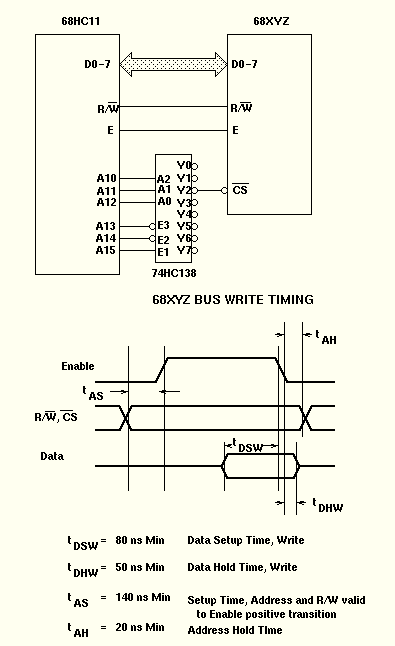
- Is
 compatible with the 68HC11? Why or why not?
What is the corresponding time for the 2 MHz 68HC11?
compatible with the 68HC11? Why or why not?
What is the corresponding time for the 2 MHz 68HC11?
From Figure A-14 of the Technical Data Manual, corresponding time is 3 - 19,
or 222 ns - 128 ns = 94 ns.
HC11 puts data on bus 94 ns before E goes high, STUPID needs it 80 ns before,
so time is compatible.
- Is
 compatible with the 68HC11? Why or why not?
What is the corresponding time for the 2 MHz 68HC11?
compatible with the 68HC11? Why or why not?
What is the corresponding time for the 2 MHz 68HC11?
From Figure A-14 of the Technical Data Manual, corresponding time is 21 - 9,
or 33 ns - 33 ns = 0 ns.
HC11 removes data and address at same time, STUPID needs address on 50 ns
after data removed, so time is not compatible.
- Is
 compatible with the 68HC11? Why or why not?
What is the corresponding time for the 2 MHz 68HC11?
compatible with the 68HC11? Why or why not?
What is the corresponding time for the 2 MHz 68HC11?
From Figure A-14 of the Technical Data Manual, corresponding time is 12,
or 94 ns.
HC11 puts address on bus 94 ns before E goes high, STUPID needs address on
140 ns before E goes high, so time is not compatible.
- Is
 compatible with the 68HC11? Why or why not?
What is the corresponding time for the 2 MHz 68HC11?
compatible with the 68HC11? Why or why not?
What is the corresponding time for the 2 MHz 68HC11?
From Figure A-14 of the Technical Data Manual, corresponding time is 9,
or 33 ns.
HC11 holds address on bus 33 ns after E goes low, STUPID needs address on
held for 20 ns before E goes low, so time is compatible.
- Explain in words what
 means.
This is the amount of time STUPID needs valid data on bus before E goes low.
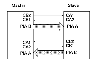
- How do you clear flags on the MC6821?
Read the port for which the flag is set.  For example, if IRQA1 is set,
read EXP_PORTA.
- Write some C code which will set up PIA Port B on the master HC11 so
that:
- The master PIA Port B is an output.
- The master CB1 is an input, active on the falling edge, with interrupt disabled.
- The master CB2 is an output, goes low on a write to PIA Port B, and goes back high on the next E clock.
EXP_CRB  = 0x00;   /* Access DDRB */
EXP_DDRB = 0xff;   /* Make Port B output */
EXP_CRB  = 0x2c;   /* CB2 control = 101; DDRB access = 1; CB1 control = 00 */
- Write some C code which will set up PIA Port A on the slave HC11 so
that:
- The slave PIA Port A is an input.
- The slave CA1 is an input, active on the falling edge, with interrupt enabled.
- The slave CA2 is an output, goes low on a read from PIA Port A, and goes back high on the next E clock.
EXP_CRA  = 0x00;   /* Access DDRA */
EXP_DDRA = 0x00;   /* Make Port A input */
EXP_CRA  = 0x2d;   /* CA2 control = 101; DDRA access = 1; CA1 control = 01 */
- Write some C code for the master which will write a byte to the slave
and wait for the slave to acknowledge receipt of the data.
temp = EXP_PORTB;             /* Make sure flag clear by reading port */
EXP_PORTB = data;             /* Write data to port */
while ((CRB & 0x80) == 0) ;   /* Wait for acknowledgement */
 C to 255
 C) which tells the SOTC-001 what temperature to set
the oven at. It then reads a byte from the SOTC-001, which tells the HC11
the actual temperature of the oven. The HC11 then deselects the SOTC-001.
The figure shows the SPI timing information. The maximum SCK the SOTC-001
can use is 250 kHz.
C) which tells the SOTC-001 what temperature to set
the oven at. It then reads a byte from the SOTC-001, which tells the HC11
the actual temperature of the oven. The HC11 then deselects the SOTC-001.
The figure shows the SPI timing information. The maximum SCK the SOTC-001
can use is 250 kHz.
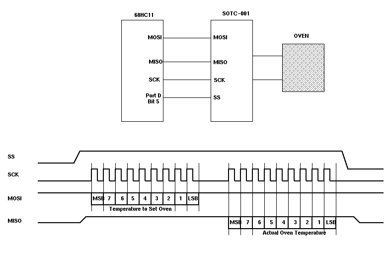
- How do you clear the SPI flag?
Read SPSR, then read from or write to SPDR.
- Write some C code to set up the 68HC11 SPI for use with the SOTC-001.
Be sure to set up DDRD and SPCR correctly, and explain what the bits you set
in SPCR do.
DDRD |= 0x38; /* SS, SCK, MOSI outputs; must do this before setting up */ /* SPCR */ SPCR = 0x56; /* SPE = 1, MSTR = 1 */ /* CPHA = 1 -- Data stable on 2nd clock edge */ /* CPOL = 0 -- latch data on falling edge */ /* SPR[1:0] = 10 -- 125 kHz clock (fastest compatible with */ /* SOTC-001 */ - Write some C code to set the oven temperature at 198
 C, and read the
actual oven temperature.
C, and read the
actual oven temperature.
PORTD |= 0x20;      /* Select SOTC-001 */
temp = SPSR;        /* First step in clearing SPIF */
SPDR = 198;         /* Writes to SOTC-001 and finishes clearing SPIF */
while ((SPSR & 0x80) == 0) ;  /* Wait for transfer to finish */
SPDR = 0x00;        /* Write dummy byte to SOTC-001 to get SCK going; */
                    /*   Also clears SPIF */
while ((SPSR & 0x80) == 0) ;  /* Wait for transfer to finish */
oven_temp = SPDR;   /* Read oven temperature from SOTC-001 */
PORTD &= ~0x20;     /* Deselect SOTC-001 */