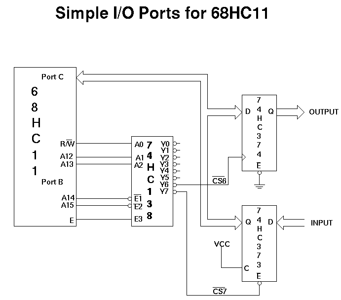
- The data setup time for the 74HC374 output port? (I.e., the time from data valid on the data lines to CS6 going high.) Does this meet the specification from the HC11 Technical Data Manual?
- The data hold time for the 74HC374 output port? (I.e., the time from CS6 going low to data being removed from the data lines.) Does this meet the specification from the HC11 Technical Data Manual?
- The data setup time for the 74HC373 input port? (I.e., the time from data valid on the data lines to E going low.) Does this meet the specification from the HC11 Technical Data Manual?
- The data hold time for the 74HC373 input port? (I.e., the time from E going high to data being removed from the data lines.) Does this meet the specification from the HC11 Technical Data Manual?