Lab 6: DIODES AND ZENER DIODES CIRCUITS
The purpose of this lab is build and test some interesting non-linear circuits.
Zener Circuits
1. Construct a simple voltage regulator (similar to figure 3.34 in Sedra and Smith) to produce 8.2 V from a 15 Volt source, using your 1N5237 zener. Make the zener current equal to 20 mA, approximately. Sketch circuit and measure the output voltage with your digital multimeter.
2. Apply a 1 K load to the regulator and measure the voltage change. What incremental zener resistance rz = Delta vz/ Delta iz does this imply? Compare with spec.
3. Apply a 100 ohm load to the regulator. What happens, and why? In theory, what is the smallest load resistance that could be applied and still have the regulator output at approximately 8.2 volts? Test.
4. How much does the output voltage change when the supply voltage is varied from 13 to 17 volts with the 1 K load in place? What percentage regulation Delta vout / Delta vin does this correspond to? Calculate this regulation from rz.
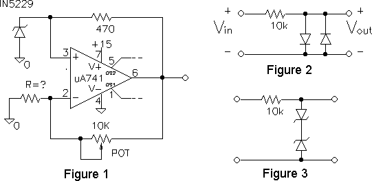
5. The circuit in Figure 1 can be used as a precision voltage source (Horowitz and Hill, second ed., Fig. 6.21). In this circuit, the source of voltage for the zener regulator is the precision output voltage. The precision voltage is obtained by amplifying the zener voltage. Note that the -V connection of the op amp is connected to ground instead of -15 V. (This is to prevent the bootstrap circuit from turning the diode on in the forward direction.)
Limiting, Clipping, Clamping, and Doubling Circuits
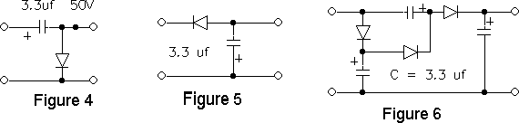
6. Construct the double diode limiter (shown in Figure 2) using IN4001's. Describe the output for a 1 V amplitude sine input. Use the X-Y mode to plot the transfer function. Observe both input and output on the same scale and note why the circuit is called a clipper.
7. Use two 4.3 V zeners in series as shown in Figure 3. With a larger input what does the circuit do? Plot the transfer function. Explain the transfer function (knowing the the zener voltage at 0.1 mA helps).
8. Construct the clamped capacitor circuit, Figure 4, making sure the polarity of both the capacitor and the diode are correct. Test it with 4 v peak-to-peak sine input. Describe the effect of the circuit (account for the voltage drop across the diode in your explanation). Add an offset to the sine input, what is the effect? Why?
9. Keep the clamped capacitor circuit and build the rectifier (Figure 5). Measure and explain the output of the rectifier, when the input is a 4 V p-p sine from the signal generator. Next use the output of the clamped capacitor as an input to the rectifier. (Figure 4), sketch the total circuit. Measure and explain the output. What would you call this circuit?
10. Extra credit. Construct the circuit shown in Figure 6. Keep the input at 4 V peak-to-peak and measure the voltage at each node. What does it do? Explain how it does it. What would you call this circuit?