EE 321 Lab
Lab 8: BIPOLAR JUNCTION TRANSISTORS, Part I
Prelab for Lab 8
In this lab we will investigate how a bipolar junction transistor
(BJT) can be used to amplify signals.
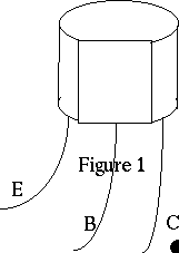
1. First, use your multi meter to measure
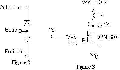
the base-emitter and base-collector junctions of your transistor (Figure 1 and 2).
Put the meter in ``Diode'' mode (a picture of a diode shows),the meter indicates
the voltage for 1 mA current when forward biased and 0 if reversed biased.
Test the method on a diode then on a 2N3904 transistor.
Record your readings. This is a useful way to check for bad transistors.
This is better than using the Ohm-Meter for measuring the forward and
reverse resistances of the junctions, as the measuring voltage and current
are not known.
2. The basic principle of a BJT is that the base-emitter voltage
vBE controls the collector current iC, when
the transistor is
biased in its `active' mode (b-e forward biased, c-b reverse
biased).


-
Construct the circuit (Figure 3). Lay your circuit out
neatly as it looks on the schematic, between the bus
lines for VCC and ground.
- Connect a sine wave to vS and display vBE and
vC in on your oscilloscope.
- Adjust input sine wave, vS (the d.c. bias (offset) and amplitude)
so that vBE varies from about 0.0
to about 0.73 volts. Be sure to measure vBE at the base of the transistor. Make vBE big enough that vO goes
from 10 V to 0 V.
- Both vBE and vO will look like clipped sine waves.
Where do they clip?
3. Note that vC = VCC - iC RC.
Use this to determine where the transistor is in cutoff (iC = 0)
and where it is in saturation (vCE less than 0.7).
(In between, the transistor is in its active region).
-
Display vC vs. vBE in the x-y mode.
Using this curve, plot iC vs. vBE.
THIS CURVE SHOULD LOOK like
figure 4.12 in Sedra and Smith.
Note the three regions on the plot
-
For what value of vBE does the transistor start to turn
`on'? (Collector current start to flow?) Does this make
sense?
-
When vBE is too large, the collector current will drop vC
below vB, thus forward-biasing the collector-base junction
and driving the transistor into saturation. For what values
of vBE and iC does this occur?
4. The transfer characteristic is linear if vBE is restricted to small
changes about a bias point, as in Figure 4.24.
-
Reduce the p-p signal
amplitude and change the offset until only a small part of the transfer curve going from about 3.5 mA to 6.5 mA is left (fiddle with the signal
generator until the output is a sine wave that goes between 6.5 V
and 3.5 V. Start with an input amplitude of 0.1V and offset of 0.5v).
Now you should find that vC changes by 3 V
p-p about the bias point at IC = 5 mA.
-
Sketch the operating range on the plot of part 3 above.
-
In the time domain, display vBE and vC on your scope.
What is the voltage gain vc / vbe for
the small signals? (Be sure to measure the `input' vbe
after the 10 kOhm
resistor.)
-
How does the gain compare with theoretical value found in the prelab?
5. How could the gain be made larger? (There are two ways.)
6. Increase vBE and note the distorted nature of
vC. Increase vBE further until the output just
"clips" on top and bottom. (Readjust the d.c. level so that the
clipping is symmetrical).
- Sketch a clipped waveform.
-
Note the
d.c. levels of the clipping, and whether the clipping is due to
saturation or cutoff.
7. The output voltage can be linearized over its entire range by using
the input signal to control the base current rather than the base
voltage. This is because the collector current is proportional to
the base current, i.e. iC = beta iB. We will show this in the
following way:

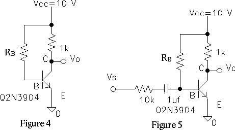
First we will bias the transistor in its active state by supplying
a current to the base through RB from +VCC
(see Figure 4). This provides
a d.c. base current IB = (VCC - 0.7V)/RB, which gets
amplified by the transistor to give a d.c. collector current
IC = beta IB. Because beta varies from transistor to
transistor you will have to select the value of RB to obtain the desired
IC.
-
The desired current for IC is 5 mA
-
Begin by assuming beta=100 and calculate RB.
-
Use this RBin the circuit, measure IC, and then
get a better estimate of beta.
-
Repeat this step until IC = 5 mA +- 0.5 mA.
-
What value of RB did you need, and what value of beta does
this imply?
8. Now add a signal component to the base current through a coupling
capacitor, as shown in Figure 5, which does not affect the d.c. bias. Note
that the input voltage has been converted to a current by resistor RS.
-
Increase vs until the output clips, and back off
until the clipping just stops.
-
What is the maximum output voltage swing
-
Is the output linearly related to the input. vs? (Adjust the scope -position,
sensitivity, invert- until the input and output line up. If they line up
and the output is a bigger copy of the input they are linearly related.)
-
What is the voltage gain, vout / vs?
9. EXTRA CREDIT. The theoretical signal gain is determined from the
expressions vout = - ic RC,
ic = beta ib, and ib = vin / RS.
where all the currents and voltages are changes from their bias
values caused by the signal.
-
Solve these equations for the
signal gain vout / vin.
-
Use the measured value of the gain to
estimate beta again.
-
How does this value of beta compare with the value
determined in part 7?
© Copyright 1996 New Mexico Institute of Mining and Technology
