EE321 Lab #11
MOS FIELD EFFECT TRANSISTORS (MOSFET's)
Prelab for Lab 11
The purpose of this lab is to investigate the characteristics of MOSFET's,
and to use them in some simple circuits. For simplicity we will use only
n-channel devices.
Static Characteristics
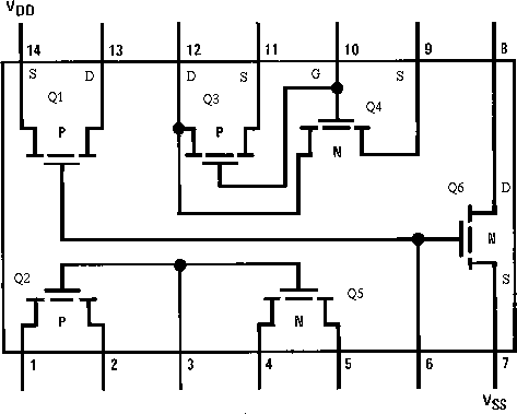
1. The CMOS 4007 integrated circuit contains 6 enhancement MOSFET's, 3
n-channel and 3 p-channel. The n-channel bodies(p-silicon) are connected
to pin 7 and must be kept at the most negative voltage used in the
circuit. The p-channel bodies (n-silicon) are connected to pin 14 and
must be kept at the most positive voltage used in the circuit. The drain
and source are interchangeable on Q2 and Q5.
-
WARNING! Although there are protection diodes connected to the
input pins to minimize damage from static charge, TWO OUTPUTS ARE NOT
PROTECTED.
ANTI-STATIC PRECATIONS MUST BE TAKEN.
Be very careful. Use wrist strap when hanhling and inserting
into the board. Make sure all connections are correct before turning
on the power. Ground all unused inputs. Keep your chip in the static bag
when not in use. Do not change connections with power on.
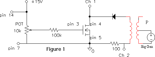
Connect pins 7 and 14 to the correct voltages.
- Build the circuit and set the inputs to measure
iD and vDS in the pinch-off region for
one of the n-channel devices (Q5, pins 3, 4, 5) using the circuit shown.
With the gate voltage set to about 5 V, adjust the signal generator to a triangle
wave with maximum amplitude at 1 kHZ.
Be sure to connect pin 7 to ground and pin 14 to
+15 V. iD is proportional to the negative of the voltage across
the 100 ohm resistor, ch 2 inverted. Now increase the gate voltave untill
current is flowing in the MOSFET.
- Display iD vs. vDS for the n-Channel FET. Measure
Vt by varing the gate voltage untill current just begins to
flow in the drain circuit (increas the sensivity of the scope to get a good measurement).
Carefully draw the characteristics for one of the transistors at 4 values
of vGS. Label your axes.
- Find k'W/L from each these curves in the saturation region. If the value
of k'W/L is much different for each of these vGS, measure
Vt again, more carefully.
2. Does the MOSFET behave as a variable resistor for small drain-source
voltages (both positive and negative vDS)?
-
Find the resistance (from your measurements of the slope with average vDS
= 0 ie no offset) of the MOSFET for small vDS values when
vGS = Vt+1. Compare with theory (Sedra and Smith
eq. 5.13).
-
Find the resistance for vGS = 0 V and 15 V.
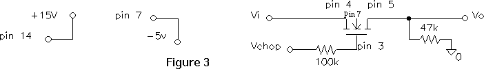
Voltage Controlled Switch
3. Construct the following "chopper" circuit, which uses a
square wave across the gate-source to turn the MOSFET on and off. The path
from the drain to source acts as a resistor in a simple voltage divider.
The resistance is very high for off and low for on.
-
Note that pin 7 must be connected to -5 V so that vi can go negative.
-
Set vi to a 2V p-p sin at 1 kHz and vchop to a square wave from -10 to +10V at 100Hz. Sketch or copy the output.
- Change vchop to 10 kHz and sketch or copy the output.
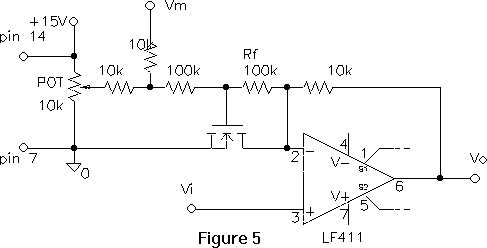
Variable Gain Amplifier
4. The gain of the following amplifier can be controlled by the gate
voltage on the FET, which is supplied by a voltage divider. Construct the
circuit and apply a small input voltage (less than 50 mV p-p) at 1 kHz.
How much can the gain be varied, and does this agree with the range of
resistance values for the FET?
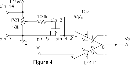
5. With the gain of the amplifier at approximately 5, increase the input
signal amplitude until the output distorts noticeably. Can you figure out
what causes the distortion? Sketch a distorted waveform.
6. Extra Credit. The distortion can be reduced dramatically by feeding
half of the drain voltage back to the gate with Rf, as shown.
Connect a 1 V p-p sine wave as shown to vary the gate voltage. The amplifier
output should be an amplitude modulated signal.
 © Copyright 2000 New Mexico Institute of Mining and Technology