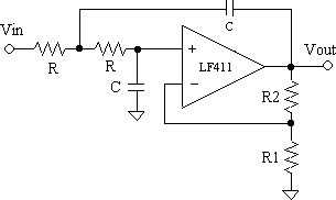
- First test the amplifier without the filter by first measuring its low-frequency gain and comparing with what the gain should be. NOTE: the resistors for the amplifier are not equal to each other or to the filter resistors.
- Confirm that the filter has a low-pass frequency response and measure its cutoff or 3-dB frequency fc. For a Butterworth filter, the 3-dB cutoff frequency should be the same as the pole radius, i.e., w0 = wc. Is it?
- What is the low frequency gain, and how does this compare to what it should be?
- Measure and document the step response of the filter for comparison with later results. Does the step response overshoot? What is the gain after the transient response dies out, and what should the gain be?
- Sketch the pole locations of this filter, approximately to scale.
- What are the effects of varying the pole locations on the step response of the amplifier? Document for the particular cases of a Bessel filter (K = 1.268) and a 2.0 dB Chebyshev filter (K = 2.114). Don't change the R's and C's that determine fc.
- Observe the frequency response (measure and plot the gain at each kHz from about 1 to 15 kHz) of the 2.0 dB Chebyshev filter. Why is it peaked? The peaking constitutes the `ripple' of the (frequency response of the) filter. Is the ripple equal to 2.0 dB? Measure the 3 dB cutoff frequency and compare with the theoretical value obtained from fn = 0.907. (fn = f0 / fc f0 is determined by RC, and fc is the 3-dB frequency) Why is the cutoff frequency larger than the pole radius? Illustrate using a sketch of the pole locations similar to that of part 1.
- Measure and plot the frequency response and fn for the Bessel filter and compare with theory. Does the Bessel filter have ripple? Sketch its pole locations, as before.
- Measure and plot the frequency response and fn for the Butterworth filter and compare with theory and the other filters. Does the Butterworth filter have the flatest responce?