EE 322
Lab 6: THE 555 TIMER
The purpose of this lab is to investigate the use of the 555 timer integrated
circuit as an oscillator and as a monostable multivibrator for generating
pulses and delays.
The 555 timer uses two comparators and a digital flip-flop to control
an output driver and a `discharge' transistor (see sketch below). The comparators
switch state at 1/3 and 2/3 of the supply voltage (Vcc), called
the `trigger' and `threshold' levels respectively. When the trigger input
(Tr) falls below (1/3) Vcc the output voltage goes high and
the discharge transistor behaves like an open switch. When the threshold
input (Th) rises above (2/3) Vcc the output goes low and the
discharge transistor shorts the discharge terminal (pin 7) to ground.
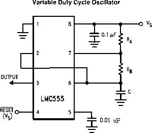
Astable or relaxation oscillator
When connected as shown below, the 555 functions as an `astable' (unstable) multivibrator
or `relaxation' oscillator. C charges up through RA and RB
until its voltage VC reaches the threshold level (2/3) Vcc.
The discharge transistor then turns on connecting the junction between
RA and RB to ground and discharging (relaxing) C
until VC = (1/3) Vcc, whereupon the discharge transistor
turns off and the process is repeated. The period of oscillation is given
by
T = 0.69 ( RA + 2 RB) C.
- Design your circuit to have an oscillation period T = 2 ms, with RA
= RB and C = 0.1 uF. Construct and test the circuit, using the
dual-trace capabilities of your scope to look at both the output and the
capacitor voltage (be sure to use d.c. coupling and keep track of 0 VDC).
Make a hard copy of or sketch the waveforms and explain them. How does
the observed period/frequency compare with the theoretically expected values?
What is the purpose of the 0.01 uF capacitor on the control voltage terminal?
Be sure to connect the reset pin to power.
- Why is the output pulse at a high level longer than it is at a low
level? Does the ratio of the charge and discharge times agree quantitatively
with your explanation?
- Short out resistor RB. How does this affect the waveforms,
and why? The slope of the discharge waveform can be used to be used to compute the current
drawn by the internal discharge transistor of the 555.
-
If you 555 IC is the BJT version,
derive an expression
for calculating the discharge current and evaluate (Hint dV/dt=I/C for a capacitor).
Assuming that the discharge
transistor has a beta of 100, what base current is supplied by the internal
RS flip-flop of the 555?
- If you IC is the CMOS version the discharge should be exponential. Use the
initial slope to find the "on" resistance of the discharge FET. Hint: the initial slope of
the decreasing exponential is Vo/RC.
- Restore RB to its original value and replace RA
by a 470 ohm resistor. What do the waveforms look like now, and why? Why
do we not short out RA?
- Vary Vcc between +5 +15 volts to see how the output frequency
depends upon the supply voltage. Does it? Use a frequency counter to measure
the frequency at 5, 10, and 15 V.
Voltage-Controlled Oscillator
Often a circuit requires a voltage-controlled oscillator, that is, an
oscillator who's frequency depends on an input voltage. The frequency of
the astable multivibrator above depends only on the values of RA,
RB and C. By using a voltage-controlled current source to charge
C, one can adjust the charging rate and hence the frequency. If a current
source charges the capacitor with a constant current I, as in the circuit
below, the time for the capacitor to charge from VTh to VTr
is
tch = C (VTh-VTr)/I = C Vcc
/(3 I).
The circuit below will discharge virtually instantaneously, so the frequency
of oscillation will be
fosc = 1 /(tch+tdis) =1/ tch
= 3 I/ (C Vcc).
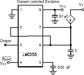
- Return Vcc to 5 V for the 555 timer.
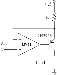
- The voltage-controlled current source below was obtained from
Horowitz and Hill (Figure 4.11). Build this current source. Use +-15 V power supplies
for the op-amp. Select R such that the frequency of oscillation will vary
from 5 kHz to 10 kHz as Vin is varied from 10 V to 5 V. Test the current
source with a resistive load of 1 k.
- Use the current source to charge the capacitor in the 555 oscillator circuit. This
should make a good saw-tooth wave.
- Vary the input voltage between 5 and 10 V. Record and plot fosc vs. Vin.
Monostable Operation
The circuit shown below produces an output pulse whenever the trigger
input (Tr) falls below (1/3) Vcc. The duration of the output
pulse is T = 1.1 RA C. After this time the output remains `stable'
at 0 volts until the next trigger pulse occurs.
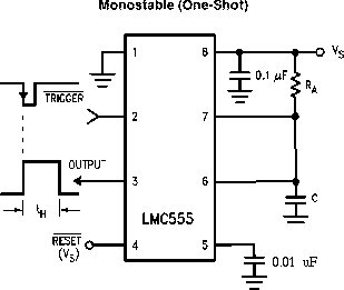
- Design the circuit to have a 1 ms pulse length and trigger it with
short-duration, negative-going pulses as shown.
- The input trigger signal can
be obtained by appropriately setting your pulse or signal generator.
Look at the pulse from the signal generator with the scope to adjust it.
A good pulse signal would be 100 Hz going from 5 V to 0 V for 0.1 ms each cycle.
- Look
at the output and capacitor waveforms. Sketch or copy and explain.
- Measure the output pulse width and compare with its theoretical value.
Vary the width of the trigger pulse to determine its effect upon the output
pulse width, and describe the results.
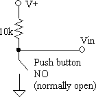
- The monostable can be used to generate long time delays by increasing
the values of RA and C. Try generating a 10 second delay (pulse)
using a l00 uF electrolytic capacitor. Trigger the circuit manually as
shown below. The
switch can be just a wire you touch to ground to start the 10 second pulse.
- How does the pulse length compare with theory? (Note: You
can use a long time base and the `scroll' mode on your digital scope to
watch the capacitor charge and to measure the time delay.)
© Copyright 2003 New Mexico Institute of Mining and Technology