EE 101
Pre-Lab Exercise 11
In this lab we will implement a 4-bit couter that counts from 0 to F in hex repeatedly and displays the count value on a 7-segment LED display. For each hex value you will need to determine which of the 7 LEDs need to light up to display it. For the prelab, complete a truth table for the MAN74 seven-segment LED. To do this you'll need to make a truth table (like the one started in class last week) with a column for each bit in the 4-bit counter (A, B, C, D), a column for the corresponding hex values (0 through F), and a column for each of the outputs a through g which drive the LEDs in the MAN-74. A HI signal turns on the LED, a LO turns it off. You will need to fill in ones and zeros in the a through g columns corresponding to which LEDs need to be lit to display the desired symbol.
(end of pre-lab)
EE 101
Lab Exercise 11: 4-Bit Counter/Decoder/Display
This purpose of this lab exercise is to familiarize you
with the Altera/Quartus programming environment's ability to link two or more
design files together into a larger master design. You
will create a circuit which will integrate a 4 bit counter (from a graphics
design file) with a decoder (from a text design file) into a new project to control a MAN74 7-segment LED display. You will demonstrate the MAN74 counting from 0 to F repeatedly, with direction selection (counting up or down) and reset control.
There are a few important considerations for this lab:
- For this lab you will need to be careful to switch projects when you start on a new one. If you finish a project and start a new file for a new project without setting a new project name your new file will be associated with the old project! Generally it is safer to just quit the Quartus program completely between projects.
- You should make a new folder for today's lab and a subdirectory within for each of today's three projects (couter, decoder, lab11).
- This lab assumes you remember, or can go back and look up, the procedures we used for last week's lab 10. Here we will highlight what material is new, namely the integration of several projects into one master project, while much of the creation of the individual component projects will be review from lab 10.
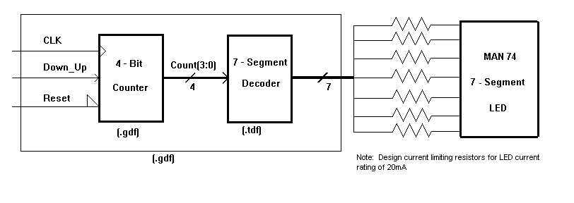
Figure 1: Block Diagram for 0 to F Counter/Decoder/Display
Part I
In this part of the lab, you will create a graphics design
file for a 4-bit counter.
- Create a separate directory called "Lab11" which you will use as the working directory for this lab. Be sure to save all your work from this lab into this directory.
- Load the Quartus software and create a new project. Use "counter" for the
project name in Part I of this lab. Use the same specs as last week, including the device type EPM7064SLC44-10.
- Create a Block Diagram File which
will define the 4-bit counter. Altera provides primitives and macrofunctions
that you can use in your design file.
- First, create a new file by choosing New from the File menu. Select Block Diagram/Schematic File This will have a .bdf extension. and OK. An untitled Graphic Editor window opens.
- Now is a good time to name this file, so choose File:Save and by default it will give this file a name that matches your project name. Note: The file name and project name must have the same prefix. In this case, the file name should be counter.bdf, and you should put it in a folder called "counter".
- Place the counter device symbol in your design. This will insert the a 4-bit ripple counter.
- Edit: Insert Symbol (or double click in white work space). A "Symbol" window open.
- Choose "Others" library then "MAXPlus2" folder.
- Scroll down and find "4count", select it and click OK. (For future reference, you can simply type "4count" in the Name box without searching the library.)
- The 4COUNT symbol is now attached to the mouse cursor with its upper left corner at the insertion point. Use the left mouse button to place it on the page. Notice that the symbol is outlined in blue to indicate that it is presently selected. Deselect it by clicking the mouse outside of the selected symbol. In a bdf file the snap-to function is automatically enabled to help you align symbols on the page. Adjustments for this behavior are possible but in general you shouldn't need to change them.
- Now you are ready to create your input and output pins. The counter you are working with requires these signals to be attached to it: clock, count direction (down or up) and the 4-bit output. There are other pins located on this counter, but for this lab we will not require them. To enter the required signals on your schematic:
- Double-click the mouse in a blank part of the work area to display the Enter Symbol dialog box. Type "INPUT" in the Symbol Name box, and choose OK. A generic INPUT symbol is displayed. (Rather than typing the name you can find the input pin in the "Primitives" library, "Pin" folder.)
- Repeat this process so that you have a total of 3 input signals (or simply copy and paste the input symbol 2 more times), and place them to the left of the 4count symbol
- Create four OUTPUT pin symbols using the same method you used for inputs. Place them to the right of the 4COUNT symbol.
- Name the input pins.
- Point to the default pin name "PIN NAME" of one of the input symbols and double click the left mouse button. "PIN NAME" will become highlighted. Type "Clock" as a replacement for "PIN NAME".
- Similarly, name another input symbol "Down_Up". This signal will allow you to control the direction the device counts.
- Name the last input symbol "Reset" for the counter's clear input.
- Name the output by clicking on the output's "PIN NAME" as you did for the inputs. Since they correspond to the four count bits, label each one by the bit number: Count0, Count1, Count2, and Count3.
- Connecting the pins
- Connect the inputs to their proper pins by simply dragging the input pin and moving it over to touch the appropriate pin stub on the counter. Be sure they butt up to each other without overlapping to get the connection made. Drag the pin away slightly to confirm that there's a wire connecting it. If this doesn't work, be sure the Use Rubberbanding button is selected and the Use Partial Line Selection button is turned off (these are found on the vertical toolbar along the left margin of the page).
- Repeat for the other input signals. "Down_up" connects to DNUP, "Reset" connects to CLRN, "Clock" connects to CLK. If you want to move the inputs around for readability, a wire will automatically be drawn as you drag input and move it. (This is the rubberbanding feature, which is on by default). The signals should now be attached to the proper "4COUNT" pins.
- Do the same for your output pins. Be careful to connect them in the proper order. Count0 is our least significant bit (LSB) while on the 4count symbol the LSB is QA. So connections should be as follows: Count0 to QA, Count1 to QB, Count2 to QC, and Count3 to QD.
- Compile your program. The compilation report will display when a successful compilation is achieved.
- Simulate your program:
- See last week's Lab 10 instructions for how to create the vwf simulation file. Use the default name which should match your project name "counter".
- Set an End Time of 32us (Edit:End Time)
- View:Fit in Window to show the entire duration in the window. (keyboard shortcut is Crrl-W)
- Inserting nodes into the simulation
- Edit:Insert node or bus Refer to Lab 10 for details if you don't remember how to do this.
- In the Node Finder, list nodes and "copy all" to add all of the nodes to the simulation.
- Make these modifications to your input signals (Highlight the part of signal to be modified by dragging across that portion of the timing diagram with the mouse), Edit:value or use icon buttons in the left margin of the waveform window to overwrite):
- Reset should be high until the 30.0us mark, low thereafter.
- Down_Up should be high until the 16us mark, low thereafter.
- Overwrite the clock for the entire duration of the simulation, use 1us for the period.
- Combine count outputs into a group for easy display of their combined value.
- By default these are in order of Count0 to Count3. Rearrange by dragging so they are in the opposite order from 3 to 0 (top to bottom).
- Hold the control key while clicking on each to select all four count outputs.
- Right-click on the selected outputs, select "Group"
- Name = "Count[3..0]", Radix = Hexadecimal
- The Count[3..0] now shows as a single line with the equivalent value of the count. The plus sign indicates that it is a group of signals which can be expanded/collapsed by clicking on the +/- icon. For this step expand the group so that the individual components are visible.
- Simulate: Ctrl-i or Processing: Start Simulation or use the blue ~> play icon.
If you encounter a warning about not having an input file specified in the settings window, do the following steps (sometimes this is done by default, sometimes not):
- Assignments: Settings click on "simulator settings"
- Click the "..." button next to the "Simulation Input" box
- Select "all files" in the "File Type" box
- Locate the .vwf file that matches your project name (counter) and select it, click OPEN
- Click OK to close the counter settings window
- Save and simulate
- Verify that the counter is working correctly. Observe the count values and see that it reverses and resets when the Down_Up and Reset inputs change. In most cases this simulation time will show a count starting at 0, counting down to zero then back up to E, then reset to zero. If you want to see a longer sequence you can extend the end time and move the time of your reset.
- Print out a copy of your block digram and simlulation report files and paste them in your notebook. The default settings usually work fine for this.
- Create a symbol from your bdf file: The .bdf file you have just created will be incorporated into another project later. In order to do this, you will have to create a Block Symbol File (.bsf) that represents this creation. The symbol you create can be used like any other macrofunction symbol in a block diagram file that is at a higher level in the project hierarchy. To create this symbol:
- Click the counter.bdf tab to display the bdf file.
- File: Create/Update: Create symbol files for current file
- Click OK to the creation message. Your symbol file has been created. For some types of design files, a symbol may have been created when you first saved the file. If so, you will get a message asking whether it is OK to overwrite the existing symbol. Choose OK to ensure that you have the most up-to-date information in your Symbol File.
- That concludes this project. You must close this project before you start another, generally the best way to ensure this is to quit the Quartus program and start over from scratch in Part II.
Questions for Part I:
- When setting up your simulation file, how does specifying "groups" instead of "outputs" affect the data provided by the simulation?
- Describe how the reset signal affects the output of your counter.
- Describe what happens when the Down_Up signal is toggled.
Part II
In this section we're going to build a decoder that translates the 4-bit counter value to the proper 7-bit a through g outputs necessary to drive the 7-segment LED display. The inputs to this system are the Count0 through Count3 outputs from the counter you just built in Part 1, the outputs are the LED channels a through g.
We need to start a new project at this point, so if you didn't exit out at the end of part one, quit Quartus and re-open it. At this point, you should not have any files open on the Quartus desktop. (You can also start a new project and it will ask if you want to close the old one. Just BE SURE you do not do the next steps while still in the previous "counter" project.) Refer back to lab 10 and part 1 above to recall how to do these steps.
- Create a new project and name it "decoder" which is the name you will give to the files within the project as well, and store them all in a folder called "decoder".
- Create an AHDL text design file to define the truth table for a hexadecimal to seven segment LED decoder. Follow the example in Figure 2 when creating this file. The beginning and end of the file have been provided, you will need to fill in the decoder rows according to the table you generated for the prelab.
SUBDESIGN decoder
(
Count0,Count1,Count2,Count3 :INPUT;
a,b,c,d,e,f,g :OUTPUT;
)
BEGIN
TABLE
Count3, Count2, Count1, Count0 => a, b, c,
d, e, f, g;
0, 0, 0, 0 => 1, 1, 1, 1, 1, 1, 0;
0, 0, 0, 1 => 0, 1, 1, 0, 0, 0, 0;
. . . . . . .
. . . . . . .
. . . . . . .
1, 1, 1, 0 => 1, 0, 0, 1, 1, 1, 1;
1, 1, 1, 1 => 1, 0, 0, 0, 1, 1, 1;
END TABLE;
END;
Figure 2: AHDL File for Seven Segment LED Decoder
- Be sure to name your four inputs the same as you named the outputs from the counter file you created in Part I. If you don't, your files will not be able to "talk to each other" later.
- When you are finished with your decoder AHDL file, save and compile as usual.
- Simulate your decoder
- Create a vector waveform file
- When you enter nodes, select the Count0 through Count3 input nodes and outputs a through g. Remember when you group these they need to be in 3 to 0 order from top to bottom to get the LSB/MSB order correct.
- Set end time to 16us, and fit view to window (Ctrl-w).
- This time you will need to overwrite the count value with a hex count. Select the "count" input grouping and assign it appropriate values:
- Edit: Value: Count value the "Count Value" window opens
- Select "counting" tab
- Set radix to Hexadecimal
- Start value = 0000
- Increment by 1
- Select "Timing" tab
- Start time = 0
- End time = 16us
- Count every 1us
- Click OK
- Save file to default project name in the same directory.
- Simulate
- Verify that the outputs agree with the truth table you created for the pre-lab.
- Print out a copies of your AHDL and simulation files and paste them in your notebook
- Have a lab assistant verify your results before proceeding.
- Create a symbol file for this decoder like you did for the counter in Part I.
Question for Part II:
- What is the obvious advantage for using a truth
table format as opposed to Boolean equations for every output when designing
an AHDL file to decode binary numbers to a 7 segment display?
Part III
Now that you have created both of the necessary symbols, you will next link them together in a new project. To close the old project, quit the Quartus program and restart, or you can create a new project and click YES when it asks if you want to close the old one. Again, just be certain you are not still in the decoder project.
- Create the new project:
- File: New Project Wizard
- Select the directory for today's lab, then the one within called "lab11", name the new project "lab11", and click NEXT.
- Add both design files to this new project.
- Click the "..." button next to the "File Name" box.
- Locate directory where decoder.tdf file is stored and select the file.
- Click "Add" when returned to the Add Files window
- Repeat this process for the counter.bdf file.
- Click NEXT
- Select device from the MAX7000S family: EPM7064SLC44-10
- Make the new .bdf file
- File: New Block diagram/schematic file
- Insert symbols for the counter and decoder
- Edit: Insert Symbol
- Click on "..." button next to "File Name" box.
- Navigate to the directory where you put the counter symbol (same as project directory) and select "counter.bsf"
- You will see a picture of the symbol in the "Symbol" window, click OK.
- The symbol for the counter will be attached to the cursor. Place it on the workspace.
- Repeat this process for the decoder.bsf symbol file, placing it to the right of the counter symbol.
- Place 3 input pins (Down_up, reset, clock) and 7 output pins (a, b, c, d, e, f, g). Look back to Part I to review this process if necessary.
- Connect Count0, Count1, Count2, and Count3 on the counter to the same pins on the decoder. Use the line drawing tool (icon looks like a right angle with boxes at the ends, use the thin version)
- Have the TA or instructor verify this before proceeding.
- Compile and save
- Simulate
- Create a new vector waveform file
- Insert appropriate nodes, we only need the three inputs (Down_up, reset, clock) and 7 outputs (a, b, c, d, e, f, g).
- End time = 32 us
- Fit in window (Ctrl-w)
- Set clock line to clock values, period = 1us
- Double click on reset and make it value 1 from start time 0 to end time 30 us, 0 thereafter
- Set Down_Up high for the first 16 us, low thereafter
- Simulate (Ctrl-i) and verify that the device counts correctly for the stated input conditions. Watch that it changes counting direction when the Down_up input changes, and that it resets when the reset input changes. Also be sure it outputs the correct series of values to feed the LED display according to your prelab truth table.
- After you are satisfied that it is correct, print a copy of the simulation results and the Block Diagram file for your lab book.
- Also print out the pinout table for wiring reference.
Question for Part III:
- List some advantages of creating and simulating a design project in separate parts (like the first two parts in this lab) instead of all in one design file.
- Why are you being asked to simulate (and verify) each part of this project before you proceed to the next section?
Part IV
Build and test your counter circuit on a protoboard.
- Program an Altera EPM7064SLC44-10 PLD with your lab11 project.
- Build the circuit.
Connect the clock input to the TTL signal on your protoboard and set it to a frequency slow enough to observe (5 hx or so is a good place to start)
- Wire the the Down_Up and Reset inputs to logic switches so they can be changed easily.
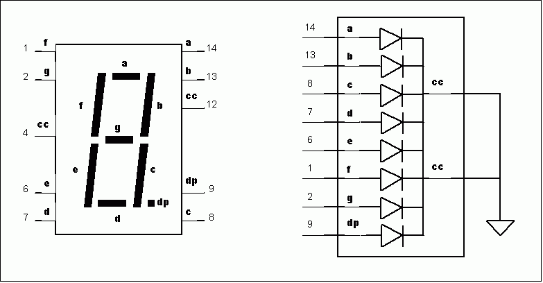
- Connect the seven outputs through current-limiting resistors to the appropriate inputs on the MAN74. The LEDs that make up the MAN74 are designed to operate at 20 mA. As such, choose any resistor values between 250W and 1KW to limit current through the LED.
- Connect the "CC" terminals on the MAN74 to ground. "DP" is the decimal point, which we do not need, but for fun you could connect it to the Down_up switch as an indicator of its state.
- After you have the counter wired and working properly, demonstrate it to the Instructor or TA and have them initial here.______
- You may now bring your chip to the demo unit at the logic analyzer station to print a waveform of your project's output. Get assistance from the instructor or TA for this part of the process. Further instructions can be found at the end of Lab 10
November 2006 | © 2006 New Mexico Tech