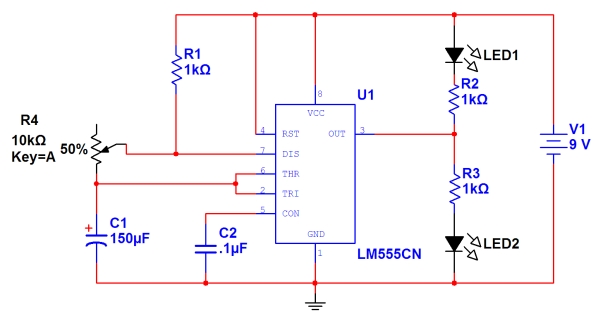
 Figure 1
EE 101
Lab Exercise 6: The 555 Timer
For this lab, you will use Multisim to simulate your design, and to verify that your design is valid. It is absolutely critical that you get a working design today, because this schematic will be used later to generate a printed circuit board for your final project. Settling for a non-working design today will result in constructing a non-functional final project!
Here is a great annimation of the 555 timer operation. Definitely check this out and see if you can correlate the annimated behavior with the material we covered in the prelab lecture. [Complements of Rensselaer Polytechnic Institute www.rpi.edu]
Part I - Designing your schematic in Multisim
- If you haven't already done so, finish the calculations in the last step of the prelab.
- Using the Multisim schematic capture program, enter the circuit that you designed in the pre-lab. Refer to Figure 1 to help you with parts placement and attributes. Below are some items to help you define certain elements of your circuit:
- The voltage source is in the Sources group, Power Sources family, and it's called DC_POWER. Place it and double click on it to assign the proper value of 9v.
- Ground is in the same group as the power source and it's called GROUND
- The 555 timer chip is in the Mixed group, TIMER family. Choose LM555CN (be sure you get the exact match).
- Resistors and capacitors can be found in the Basic group. Don't forget to select the proper value for each. It's generally a good idea to place them in the order that they're numbered on the schematic so you don't have to change that later.
- The two capacitors will come from different families. In the Family list, use CAP_ELECTROLYT for the 150 uF cap (C1). Note that it has a polarity indicator. Use Capacitor for the 0.1 uF cap (C2), which has no polarity indicator.
- Regular resistors are in the Resistor family.
- For the potentiometer (R4) use the Potentiometer family and pick the proper value from the list. Note that after you place it, when you hover over it with the mouse, a slider bar appears that you can use to adjust its value to a percentage of its maximum resistance. We will use this later to simulate the circuit for various values of R4. To ensure the potentiometer behaves as expected, you must connect to the proper terminals. Be sure to use the wiper (the terminal that becomes an arrow) and the side terminal that the wiper points toward. If you connect to the other side, the percentage adjustment will have the opposite effect. In order to orient the potentiometer as seen in the Figure 1 schematic it was flipped horizontally (after you place it, right-click on it and select 'flip horizontal').
- LED's are in the Diodes group, LED family. Use LED_red to indicate an OFF output and LED_green to indicate an ON ouput. Yes, you will have to think about this to get it right.
- Before you decide you're finished, be sure you drag each component around a little bit to confirm that it's actually connected to the node wire. The wire should stay connected and drag along with the component. If it doesn't, you need to connect the component to the node with a wire.
- Print a copy of the schematic diagram for your lab book (By this time we shouldn't have to tell you this right? It's a critical part of documenting your experiment.) Be sure to adjust the print options so that it prints in a reasonable size.
Part II - Simulating Your Design
- Perform an electrical rule check on your circuit. If this reports any errors, fix them at this time.
- We will want to see how the capacitor voltage controls the output voltage, so we will plot both of these voltages in the simulation. The hard way to do this is to look at the netlist report to determine what Multisim has named these nodes and remember this information later when you're in the transient analysis setup screen. The easy way is to add probes to those nodes so they show up in recognizable form on the setup screen.
There's a toolbar on the right margin of the Multisim workspace. On it, find the button with a yellow arrow label that has a tiny "1.4" in it. Click this button and hover over the first node you want to plot (either at pin 3 of the 555 timer or on the + side of the 150 uF capacitor). Click on the node/wire and it will attach a green probe arrow. Be sure the arrow points in the direction of the voltage drop you want to measure. If it doesn't, right click on it and select "reverse probe direction". When you add a probe it also adds a yellow data box. Drag that to an empty part of your work space so it's out of the way. Now add another probe to the other node you want to plot. To delete a probe, click in its yellow box to select it and hit the Delete key.
-
Transient Analysis
- For the first simulation we will set R4 to its minimum value. Hover over the potentiometer until the slider bar appears. Slide it until the indicator reads 0%. This sets the potentiometer to 0% of its maximum value (0 Ω). This should give us the maximum frequency output (if instead you get the minimum frequency it means you wired pin 6 to the wrong end of the potentiometer). We will simulate again later for each of the other R4 values you calculated in the prelab.
- From the Simulate menu select Analyses: Transient Analysis
- In the Analysis parameters tab set the end time to 0.4 seconds. Since we are expecting a frequency of 10 Hz for this value of R4, if we simulate for four tenths of a second then we will be able to see a llittle more than three periods of the waveform in the plot window. Later when you repeat these steps with other values of R4 you will need to adjust this end time for each simulation based on the expected frequency such that you display about three periods. Yes, you will have to think about this to get it right. :-)
- In the Outputs tab, add the voltages you want to plot. The probes you put on the schematic earlier should show up here as V(Probe1) and V(Probe2). Add them to the selected variables list. You can also do this without probes but in order to identify the proper node voltages you'll have to look them up on the net list report or rename them.
- When you are done setting up the analysis, click the Simulate button. The Transient Analysis window will open showing a plot of your voltages over time. Note how the output is high/on (Vcc) when the capacitor is charging and low/off (0) when the capacitor is discharging. In the high frequency case the discharging portion will appear to be nearly instantaneous and may simply look like a vertical line. This is because R4 is set to zero in this case so the time constant is extremely small for the discharge portion and it discharges very quickly. As you move to lower frequencies you will notice that the ON time and OFF time get closer to equal. This is because, as the R4 value increases, the impact of eliminating R1 from the discharge time constant has less and less impact compared to the size of R4
- Just as you did in the capacitor lab, use the cursors to measure one full period, then calculate the frequency. Be sure you do not inculde the first pulse in the measurement since it has a longer charge time (it has to charge all the way up from 0v instead of 1/3 of Vcc, making first cycle is longer). It will be a little tricky in some cases because the low portion of the waveform is very short at high frequencies. You can enlarge the window or zoom in if needed. Remember you can also set a different simulation end time to display more or less time in the window.
- Compare the measured frequency to what you calculated in the pre-lab. Calculate a percent difference (but you already knew that's what was meant by "compare," right?)
- Print a copy of the waveform. Remember to print four plots per page for a good printout size (File: Print Setup: Properties: 4 pages per sheet).
- For the first simulation we will set R4 to its minimum value. Hover over the potentiometer until the slider bar appears. Slide it until the indicator reads 0%. This sets the potentiometer to 0% of its maximum value (0 Ω). This should give us the maximum frequency output (if instead you get the minimum frequency it means you wired pin 6 to the wrong end of the potentiometer). We will simulate again later for each of the other R4 values you calculated in the prelab.
-
To observe how your circuit behaves with different values of R4, repeat step three above, each time trying different values for R4. The values you want to test are the ones you calculated theoretical values for in the prelab: 0Ω (which you did above), 3 KΩ, 6 KΩ, and 10 KΩ. To do this you will need to determine the proper percentage of 10 kΩ that gives you the value you need. In the first case you used 0%. Use the slider bar to adjust the potentiometer and re-simulate for each R4 value. Remember also to set the simulation end time appropriately for each run-through so you display about two or three periods of the wave form. This will allow you to make accurate measurements while still seeing enough cycles to observe the behavior clearly.
Compare all results (for each case of Rvar equaling 0, 3K, 6K, and 10K) to those you calculated in the pre-lab and print out the waveforms for each.
Next week we will build this circuit in the Analog Lab and observe its actual performance on an oscilloscope. That will provide the third set of data for comparison (today you acquired theoretical and simulation data, next week we'll acquire experimental data and compare them all to each other).
Again, be sure this circuit works successfully today because it is the first of four labs that together create your semester project. Creating a non-working schematic today will lead to a non-functional project later! Also be absolutely sure you save this work where you can retrieve it later, it will be needed to generate the artwork file for the printed circuit board you'll use to build the project.
October 2010 | © 2001, New Mexico Tech