Prelab Exercise 8
Given the following Boolean Equation:
F = ABCD + A!BC + AB!C + A!B!CD (Note:
A!BC reads "A, not B, C" and is the same as AB'C)
-
Draw and fully label a schematic using only 04's (NOT's), 08's (AND's),
and 32's (OR's).
-
Using a KMAP, derive the minimum equation for the original formula.
-
Draw and fully label a schematic from the reduced equation using only 04's,
08's, and 32's.
Lab Exercise 8: Introduction to Logic Gates
The pinout schemes for the logic gates you will be using in this exercise
are
given in Figure 1. Note that for all of these chips, Vcc = 5V (pin 14)
and GND = 0V (pin 7). Also, note that the pins that are inputs on some
chips are not necessarily the inputs on other chips!
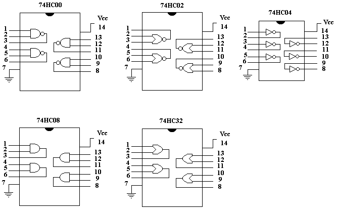 Figure 1
-
Before using these components it is helpful to understand and observe exactly what we mean when we talk about HI and LO signals, 0 and 1, Vcc and GND, +5 and 0, in logic circuits.
- Connect the 7404, 7408 and 7432 components on your breadboard to Vcc (pin 14) and GND (pin 7). This is the power they need to operate and is independent of any logic circuitry you create.
- Using connections to Vcc (for HI) and GND (for LO) as the A and B inputs to the logic chips, you will implement all the possible input combinations on each type of gate and record the observed values. Remember that a LO means 0v which is a connection to GND. LO is not the same as no connection. If you do not connect the inputs to either Vcc or GND, your IC may behave unpredictably.
- Using a multimeter, measure the output voltage (with respect to ground) of each gate for each input combination and record the measured values in the V columns of the truth tables.
- Using a logic probe, determine the logic level output (0 or 1) of each gate type for each input combination and record the measured values in the F columns of the truth tables.
| 74HC04 (NOT) |
74HC08 (AND) |
74HC32 (OR) |
| A V F |
A B V F |
A B V F |
| 0 |
0 0 |
0 0 |
| 1 |
0 1 |
0 1 |
|
1 0 |
1 0 |
|
1 1 |
1 1 |
-
The following exercises deal with the schematic in Figure 2.
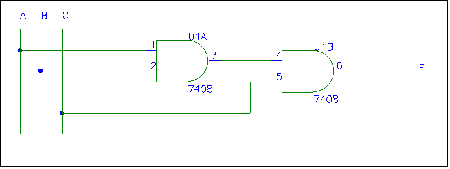
Figure 2
-
From the schematic, derive the Boolean equation for the output, F.
-
Write out a truth table based on the equation you derived in part 2a.
-
Construct the circuit in Figure 2. (Remember to hookup Vcc and ground.)
Using a logic probe, observe the values of the output for every possible
combination of input. Construct a truth table with your results.
-
The truth table you derived in part 2b should have agreed with the truth
table you observed in part 2c. If your two truth tables did not agree,
list any problems you found and what you did to correct them.
-
The following exercises deal with the boolean equation in the prelab:
F = ABCD + A!BC + AB!C + A!B!CD
-
Construct a truth table based on this Boolean equation.
-
Build the minimized version of this circuit which you reduced in the prelab.
- For every high and low combination of the inputs, test your circuit using a logic probe. The protoboard has some logic level switches you can use to easily switch your inputs. Make sure the row of switches is set to +5 (not +V), connect each input to a switch port and use the switch to select a HI or LO input.
- Construct a truth table showing your results. This truth table should agree with the truth table
you derived from the unsimplified circuit (from part 3a). If they do not
agree, find out where the problem is before proceeding.
- Don't disassemble your circuit until you have demonstrated that it works to a TA. TA INITIALS HERE _____
Questions:
-
Draw a schematic for this Boolean equation: F = A'BC + ABC' + ABC. Include
chip reference numbers (UX), pin numbers, and gate identifiers (74HCXX)
along with the inputs and output.
-
Draw a truth table for the equation in question 1.
-
How many gates (and, or and not) did your circuit require in Part 1 of
the pre-lab? In Part 3?
March 2006
Copyright 2006, New Mexico Tech