EE 101
Lab Exercise 9: Printed Circuit Board Artwork Generation
In Phase I of the class project (lab 6), you designed and simulated a circuit that would alternately flash two LED's while outputting a TTL compatible waveform adjustable from about 1Hz to 10Hz. In Phase II (lab 7) you prototyped your design on a breadboard and enhanced it to provide outputs over several other frequency ranges. In Phase III, you will scale back your design to the original specifications from lab 6 and generate artwork which will create a printed circuit board (PCB). Your design should be similar to the one in Figure 1.
There are some extremely important things to keep in mind for this lab:
- It is absolutely imperative that you have a working circuit before you move ahead with this lab. We are about to design the physical layout of your design, so if your circuit is not currently working properly, you will build a non-working project. If you had simulation trouble in lab 6, or any other problems that suggest your circuit is not 100% correct, we need to fix that NOW, or your finished product will not work.
- You can not assume your circuit is identical to the example diagrams in these instructions. There are certainly some significant differences between your schematic and the one that generated these images. Therefore you will need to identify your equivalent components by figuring out what they are connected to, rather than using the labels. DO NOT simply match up your labeled components to the same labels on the diagrams here, this will most definitely generate an incorrect layout.
I. Packaging the components
Before we convert the schematic to a PC board, we need to specify a package type for each component. This assigns a "footprint" to each component, which defines the physical characteristics including its size and shape, pin configuration and spacing, and other physical attributes. This allows us to save the appropriate amount of board space for each component when we lay out the board. It also determines where the components will penetrate the board which indicates where holes will be drilled and where solder pads will be located to attach the components.
Each component must have a footprint type defined in order to be included in the PCB design. There are several methods we can use do this, and different methods are available depending on the component type. In some cases this can be assigned in the Place Component screen when the schematic is originally created. But since we didn't do that when we created this schematic initially, we will use a combination of the other two methods. For most components, double-clicking on its schematic symbol will open a screen where we can assign carious attributes, including the footprint. For certain other components (namely the voltage source) we will need to use the footprint column of the spreadsheet view to make the assignment. And in the case of the 9v battery connector, we will need to create a custom footprint because it is an unusual part.
- Packaging the standard components
- Start the Multisim Schematics program.
- Open your design file from Lab 6, and save it under a new name (Click File - Save As) in your account. It's probably a good idea to a new folder to put it in.
- Assign a package type to each device (different methods are required for different component types):
- Resistors, Capacitors, 555 Timer, Potentiometer
- Double click on the component
- In the component attributes window, select the Value tab.
- The footprint type is listed near the bottom of the window. If you know the footprint type you can type it into this box directly. If you want to select it from a list (a safer choice), click the button to open the Edit footprint window.
- Click the Select from Database button.
- Be sure you're viewing the Master Database,
- Scroll through the list to find the appropriate footprint for each component, listed below. Be sure to look closely and get an exact match, there will be many similar-looking options. They are ordered by footprint number.
- Note that you can also just type the footprint into the
- Resistor: No. 3110 "RES10"
- Electrolytic Capacitor (150 uF): No. 1196 "ELKO13_5R5"
- Ceramic Capacitor (0.1 uF): No. 553 "CERCON1C"
- Potentiometer: No. 4342 "TO-220AB"
- 555 Timer: No. 898 "DIP-8"
- Leave the symbol and footprint pin lists at their defaults.
- When you click Select it will open a pin editor window. You will need to assign each pin on the schematic symbol to the proper polarity footprint pin. Check your netlist to determine which Symbol pin is connected to ground (Net0), this pin gets mapped to the negative Footprint pin. Most likely this will be pin 2 but there is no guarantee, you must confirm this on your netlist.
- LEDs
- Footprints for these components can only be assigned from the spreadsheet view. The default location for the spreadsheet is at the bottom of the Multisim window. If you don not see a table there, go to the View menu and select Spreadsheet View.
- Click on the Components tab below the table. A list of components now occupies the table. Scroll down until you can see the LEDs (probably named LED1 and LED2). Scroll right until you can see the Footprint column.
- Click twice on the cell for one of the LED footprints and the Edit Footprint window will open.
- Click Select from Database, be sure you're viewing the Master Database, and assign the footprint as follows:
- LED: No. 2005 "LED9R2_5Vg"
- Click Select
- Keep the default pin mapping
- Click OK
- Voltage Source
- For the voltage source (which is the 9v battery) you'll need to skip ahead to the next section and create a custom footprint, then come back to this part and assign that new footprint to the battery.
- Skip ahead to part I.B. now (just below), then come back here when finished.
- Follow the same instructions that you used for the LED, except find the voltage source in the spreadsheet (probably called V1)
- When you get to the Select a Footprint window, switch to the User Database and select your newly created 9vConnector from the list.
- Match the pins appropriately when asked. This means you must check which pin goes to ground (Node 0) on the schematic symbol in Multisim, then make sure that pin connects to pin 1 on the battery footprint (the one we designated as the minus side of the battery). It's likely the pins will be mapped 2>1 and 1>2, but you must confirm this using the netlist report or by double-clicking on the voltage source schematic symbol and looking at the Pins tab.
- Move forward to part C (skip over part B since you've already created the footprint)
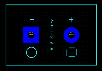
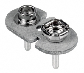
Figure 2
- Creating a custom footprint for the 9v battery: We will use a custom battery connector for this board and there is not an existing footprint in the library that corresponds to the physical layout of this part, so we will create a footprint of our own. Refer to Figure 2 for the following section.
- Open Ultiboard (it's in the same NI program group with Multisim). This is the program we use to create printed circuit boards from a schematic design. We'll do that part later, for now we're just using it to create the footprint.
- Create a new file and save it in a wise location
- Be advised that you can not re-open and edit a footprint once you have closed it, so be sure you have finished it properly before closing it. Best just keep it open for the duration of lab in case you need to go back and change something so you don't have to start from scratch if you find an error in it.
- Create footprint: From the Tools menu select Part Wizard. The part wizard step/screen numbers correspond to the numbered items below
- Select THT (through hole) and Next
- Select SIP (single in line package) and Next
- Change Units to "inch" and specify the following:
- Package dimensions X: 1.125
- Package dimensions Y: 0.75
- Next
- Ignore color settings, click Next
- Pad Type and Dimensions settings:
(The pads are spots where the components will eventually be soldered to the board. This part sets general rules for both pads, we will edit them separately later.)
- Drill hole diameter: 0.086"
- Shape: Round for top, inner and bottom
- Pad Size: Diameter: 0.2"
- Next
- Pins:
- Number of pins: 2
- Between pins: 0.5"
- Next
- Direction of pad numbering: Left-to-right. Finish
- The rectangular footprint should now be on your workspace with two round pads. We will now customize the ground pad and add some labels.
- Edit pads:
- Click the pad on the left to select it. Right click on it and select Properties
- Select the Pad tab.
- Change units to "inch."
- Be sure Copper Top is highlighted and select "Rounded Square"
- Set Rounded square radius to 0.02 inches
- Select the Attributes tab and confirm that it is pad #1. Remember this for later so we can connect it to the ground bus when we associate this pad with the voltage source in Multisim. Square pads generally indicate the low-potential side of a component or a ground connection, or in some cases Pin 1.
- Click OK
- Add labels:
- Use the layer drop-box in the toolbar (It should say Copper Top before you change it) to select the Silkscreen Top layer. This layer is the ink printing that goes on top of the board. (the copper layer contains the pads and conductive copper traces that make the board work)
- Select the Place Text "A" icon from the tool bar to open the Text window
- Change the Height to 100 mil (0.1 inch) and be sure the Silkscreen Top layer is indicated.
- In the Value box, type the text you want to add to the layer. You will repeat this process to add several references.
- Insert a minus sign "-" 100 mil tall for pin one (the square pad)
- Insert a plus sign "+" 100 mil tall for pin two (the round pad)
- Insert a part name designator "9 V Battery" (use the default 55.11811 size for this and change the font to normal).
- Arrange the labels sensibly. See figure 2. Select a label and press Ctrl-R to rotate it.
- Note that if you zoom in really close, the pin number labels will appear along with some dimensional information.
- Add icons:
- Using the circle draw toolbar button, add a circle and place it below the square pad. This circle is meant to indicate the round 'male' terminal on the 9v battery connector. Right click on the circle and select Properties. In the General tab, change the line thickness to 10 mil. Here you can also specify whether the circle is empty or filled.
- Using the line draw toolbar button, draw a dashed square to indicate the dashed 'female' terminal. You'll need to draw four 10-mil-wide lines to create this box yourself (draw a line, change its thickness like you did to the circle, then copy, paste, select, and rotate to add the rest).
- Save it in the user database
- File: Save to database
- Select User database
- Name it "9vConnector" in the window under Existing parts and click OK
- Go back to Multisim. It is advisable to NOT quit ultiboard and to NOT close the footprint design. In case you need to edit it you'll have to start over from scratch if you don't keep it open.
- Finishing the packaging process
- Assign your new footprint to the voltage source (9v battery) if you haven't already. (skip back to part I.A.3.c.)
- Look at the spreadsheet view and confirm that every component has a footprint specified in the Footprint column. If so then move on to Part II Converting the Schematic to a PCB
II. Creating an Ultiboard PCB from the Multisim schematic
Now that the preparatory work is complete we will now convert the schematic into a printed circuit board layout. We will export the Multisim work to Ultiboard. The software will keep track of what components are in the design and how they connect to each other as it converts from theoretical symbols to physical characteristics of the actual components.
- Transfering from Multisim to Ultiboard:
- With your schematic open in the Multisim program, open the Transfermenu and select Transfer to Ultiboard: Transfer to Ultiboard 11.0.
- First it will ask you to save the file. Save the file in the same new folder where your new packaged schematic. Name the file with your first and last name. YES this matters, I will need to assemble all the individual projects from the whole class into a single project to send out for production so I need to be able to easily identify your file. It would be a very good idea to use File: Save As and save new copies with incremental numbers at various stages of this project so you can backtrack easily if need be.
- When you click Save it will open the Ultiboard program and display the Import Netlist window that lists all of the components and the connections between them. If you did your packaging properly you shouldn't need to worry about this stage. Click OK.
- The new ultiboard design will appear on the screen as a jumbled mess of components. We call this the "rat's nest." The components are shown as blue outlines which represent the size and shape of the actual parts. The yellow lines indicate the necessary connections that need to be made between the component pins. The yellow box is called the keep-in boundary. This represents the actual dimensions of the finished board. The brown lines are called Force Vectors and are supposedly a tool to help in positioning components, but their usefulness is widely disputed so we will ignore them.
Your rat's nest should look similar (but not identical) to the one below in Figure 3.
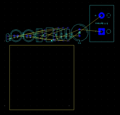
Figure 3
- Preparing the board and untangling the rat's nest:
- First we must assign the proper size to the keep in boundary (the yellow box). It is important to get this right because it is the size of board that you are allotted. Components can not be placed outside the boundary or there will be no way to attach them.
- Right-click on any keepin boundary line. It will become a dashed bold line and a shortcut menu will open.
- Select Properties
- In the Rectangle tab, change the units to inch
- Leave the X1 and Y1 alone and change the width and height both to 2.0 inches.
- Click OK and it will return you to the design window and the box will now be smaller and square, as shown in Figure 3 above.
- Next we will untangle the rat's next and place components on the board.
- One by one, drag the components into the keepin box. Arrange them by putting the battery connector in the center and placing the other components around the outside. Keep in mind that the footprint shapes may not be exact so it's a good idea to leave plenty of space around each component and to not place any component too close to the edge of the keepin box. The footprint we used for the potentiometer is only half as large as the actual part we will use so leave enough space for a part that is twice the width of the footprint.
- Components that are connected to each other directly should be located near each other whenever possible. For example, each LED connects to a current-limiting resistor. Try to place them near each other to keep the copper trace paths as simple as possible.
- Selected components can be rotated with Ctrl-R. For ease of observation it is a good idea to rotate the 555 timer (the DIP package) and the battery connector footprints (for whatever reason they usually get inserted upside-down). The other components can be rotated as needed to simplify the design.
- In general it is best to minimize the number of crossing yellow lines. This will simplify the complexity of the copper trace line routing. You won't be able to eliminate all of them but you can reduce the crossings by repositioning and rotating components.
- Be sure to leave some open space along one edge as seen on the right side of Figure 4 below. We need this space for labels in a later step.
- If you like you can try to copy the example in Figure 4, but remember yours probably won't be an exact match so don't compare the designs by component names, instead identify parts by what they connect to. Regardless, your design will differ enough to not be able to copy it exactly, rather use the sample as a guide for where to place components in general.
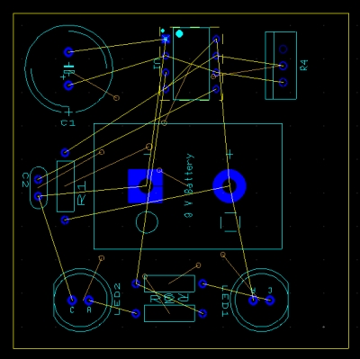
Figure 4
- Routing Traces
Once the parts are arranged on the board, each yellow connection indicator must be replaced by a copper trace line (a conductive path on the surface of the PCB) to provide the electrical connection for each node. We can do this manually but this is only possible in a reasonable time on a relatively simple board. It can be done with this board but most likely in the future you'll be designing boards that are too complex for that. Instead, we will let the software route them automatically for us.
Something to keep in mind first... the PCB is built of many separate layers. The board has a fiberglass base material (substrate) which provides the mechanical structure for the other layers. On each side of the substrate is a layer of copper which is where the conductive trace lines will be. These are sometimes called solder layers because they are typically coated with a thin layer of solder. Yes, there are two separate copper layers which is what allows trace lines to cross each other since they can run on two different planes with the substrate as an insulating layer between (more complex boards will have multiple substrates layered as insulation between additional copper layers). On top of both copper layers is a solder mask. This is the (typically) green colored layer that gives circuit boards their characteristic look. It looks like paint and insulates the copper from the outside world (except for where there are pads which are locations where parts will be soldered on). Finally, on top each solder mask there is a silkscreen layer on which we print labels, component outlines, and other useful indicators.
- Before you start routing traces, have the instructor or TA inspect your layout and approve it for the next step. This is important because it is much easier to fix layout issues now than it will be after trace lines are drawn.
- From the Autoroute menu, select Start/Resume Autorouter
- The screen will flash a few times and the yellow connection indicator lines will be replaced by red and green copper traces. Red lines represent the traces on one side of the board, and green lines indicate the traces on the other side. Yellow lines indicate places where the red and green traces cross over or run parallel to each other on opposite sides of the board. Every auto-route is unique so there is very little chance that your routes will look very much like the example in Figure 5 below.
- Now is a good time to double-check that you mapped the 9v footprint pins correctly. The square pad (the one with the circular label and the minus sign) should connect to the ground bus. You can identify the ground bus by looking for traces that link together other pins that should connect to ground, such as one pad from each capacitor and pin 1 on the 555 timer (the blue dot on the 555 timer indicates pin 1 which is also identified by a square pad). If the opposite is true then you have a problem that requires going back many steps to correct. Consult the instructor in this case.
- It is worthwhile to understand that you can re-route any traces you like. Click and drag to re-draw trace lines. They can be a little finicky so it takes some practice. You can also add additional traces but we probably have no need for that in this project so this is mentioned purely for future reference.
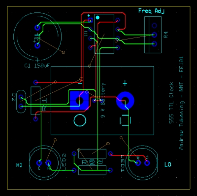
Figure 5
- Labeling the silkscreen layer
There are three labeling steps. First we will add some labels to identify the board itself, such as the name of the device and the designer's name (you!). Then we'll add some labels to assist the user such as the frequency adjustment potentiometer and the LEDs. Finally, we will add labels for the builder so they will know what components to solder in each location. Use Figure 5 above as a guide for these steps.
- Name labels
- Start by adding your name.
- We need to be sure we're working on the "Silkscreen Top" layer, so look in the drop-down box just above the workspace and confirm that's the layer displayed. If it displays anything else, switch it before you proceed.
- Click the Place Text "A" button on the toolbar. The Text window opens.
- Type your name in the Value box. After your name, it would also be good to add something to identify the class such as "NMT - EE 101" or similar. The default size in 'normal' font should be adequate.
- Click OK and it will put the text on the cursor for you to place. Put it on the edge that you left open for labels. Right-click or hit Esc to get rid of the placer when you're done. If you want to rotate the text, you must first place it then select it and press Ctrl-R.
- Now add a label for the name of the project. Follow the same process but this time make a "555 TTL Clock" label and place it near your name.
- User interface labels: Follow the same procedure as above for the following labels...
- Potentiometer:
- The text label should be something like "Frequency Adjustment" or something similar. If you like you can add + and - indicators to specify the turn direction to increase or decrease. Maybe something like "+ Freq Adj -". However, beware that this commits you to getting the potentiometer inserted such that the indicators are correct. It's hard to predict which way to insert it so we'll probably just guess, solder it in, and test it.If it's backward we'll remove it, reposition, and re-solder.
- LEDs:
- Add text labels to each LED to indicate which one is on for the HI output and which is on for the LO output. This can be determined by inspecting the traces and following one back to ground and the other back to VCC. By looking at your original schematic you can tell which one will be on in each case. YES you will have to think about this to get it right.
- Text labels should say something like "HI" and "LO". This also helps you get the LED colors in the right places. Green should indicate HI and red should indicate LO.
- Component identifier labels:
This is a step that you would normally not need to perform. However, because the instructor will be assembling all of the students' designs onto a single master board to keep the production costs low, there is an additional complication. When the instructor pastes all of these designs into a single board, Ultiboard will not be able to tolerate more than one component of the same name. Since each student has named their components by the same names, this would normally result in multiple components of each name (R1, C1, etc.). In that case Ultiboard renames the components as more designs are inserted which would make it difficult for each student to match up the parts later when it comes time for construction. Therefore, we are going to hide the component name designators that were provided with each footprint (which would otherwise get printed on the silkscreen layer), and replace them manually with text labels. That way Ultiboard's renumbering won't impact what is displayed on the silkscreen layer.
- This is a good time to save your design, then re-save it as a new name in your incremental system. That way we can return to this point easily if something goes awry.
- Start with one component and follow the process below. Then repeat that process for each component. It is important to do this one component at a time. Do not hide all of the component names at once and then expect to remember what each one was originally named!
- Double-click on the component name for a footprint (for example, start with C1). The Attribute Properties window will open.
- In the Visibility section, select Invisible. This will prevent that name from printing on the silkscreen layer without affecting the name of the part.
- Like you did for the other labels, place text that matches the component name. The default size should be adequate. In the example case the text should obviously say "C1". If you like you can also put the component value in the label to make it easy to place and replace parts. In the C1 case it should be the 150 uF capacitor so you could label it "C1 150 uF". For the LEDs you could label the color, etc. Be sure to confirm the values with your schematic first!
- The 9V battery footprint already has a text label built in so there's no need to relabel it.
- When you are done, save the file again.
III. Finalizing the artwork:
PCB creation software is generally capable of creating an industry standard set of files called Gerber files. These are universally recognized by other PCB software such that designs can be exchanged regardless of platform. Each file in the set defines the layout of each layer, plus there's another for where the holes get drilled (for inserting the components, one hole per pad). Normally you would export your project to an array of gerber files for upload to your PCB manufacturer. However, since in this case your instructor will first create a master board containing the entire group's designs, the Gerber files will not be created until after that has been done. Some day soon you'll be doing that for yourself so you'll have that to look forward to as another learning experience.
For now, you need to forward your basic Ultiboard project file to the instructor.
- First and foremost, have the instructor or TA verify that you have an adequate final design before you proceed. DO IT.
- Find the file in the location where you saved it. It will have a ".ewprj" extension. Be sure to get the latest version. Remember that the name of the file must contain your first and last name. If you ignored that instruction earlier, make a copy of it and rename it now.
- Attach it to an email and send it to your instructor. The subject line of the email should say "EE101 PCB" followed by your name. Yes it must say exactly that, with your name AFTER the required text. It might seem nit-picky but that's what allows me to sort and locate the emails easily.
- Verify that the instructor has received the file before you leave. You will receive an email reply with a confirmation code. Print it and put it in your lab book. Without the instructor's confirmation that you have completed this step you run the risk of having your project left out of the production run (and flunking a major part of the final project).
- "Being sure that you sent it" is not adequate. Really, you must verify with the instructor that the file was *recieved* before you are done!
As always, record all of this in your lab book, including printouts of your design at the relevant stages.
IV. Byte forloops and multiplex. << [nerd joke]
November 2010© 2002 New Mexico Tech