Next: 3 Supplementary Material
Up: Lab 1: HCMOS Logic
Previous: 1 Prelab
Subsections
- Use the datasheet to connect a 7404 IC.
- Verify the operation of the inverter by connecting the input to
 and
and  .
.
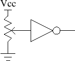
- Use a variable 10k
 pot to vary the input to the inverter.
When does the output change.
pot to vary the input to the inverter.
When does the output change.
- Build the circuit shown in Figure 1 using
10 inverters in series. Set the output of the function
generator that you build in Lab 0 to 15 kHz and connect it to
the input of your circuit. Can you observe the output of the your
circuit by using a voltmeter or a logic probe.
- Connect the output of your circuit to the logic analyzer and
record your observations. (Use the information provided in
3.1 to run the logic analyzer).
- Does the output match what you expected? Why or why not?
Figure 1:
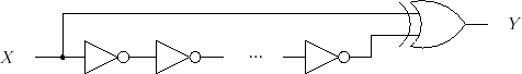 |
- What is the propagation delay of an inverter gate?
- Write the truth table for the circuit shown below.
Figure 2:
Half Adder
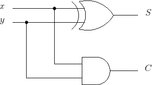 |
- Connect ICs from the 7400 family to implement the circuit shown
above.
- Verify the operation of the circuit by connecting the inputs to
different combinations of
and
.
- In terms of binary arithmetic, what do the
 and
and  outputs
represent?.
outputs
represent?.
Next: 3 Supplementary Material
Up: Lab 1: HCMOS Logic
Previous: 1 Prelab
Copyright © 2008, Electrical Engineering Department, New Mexico Tech
Last Modified 2008-09-10