


Next: 2 Lab
Up: Lab 8: Registers
Previous: Lab 8: Registers
Subsections
In this lab we will investigate two types of registers.
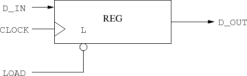
One type of register is a simple latch as shown in
Figure 1. When LOAD is high, the output data D_OUT will not change. When LOAD is low, the input data D_IN should be latched into the register on the rising edge of CLOCK.
Figure 1:
Register using simple
latch
 |
The second type of register is called a program counter (PC). This keeps
track of which instruction in memory to execute. Usually programs are
executed sequentially, so after executing the instruction at address,
say,
 , the program will then execute the instruction at
address
, the program will then execute the instruction at
address
 . In this case PC needs to increment after each
instruction is executed. Sometimes the program needs to execute code in
a different area of memory - flow control statements such as for
and while do this. In this case, the PC needs to be loaded with a new
address. In order for the program to start, you will need to reset the
program counter to zero to start execution at the first instruction of the
program. Figure 2 shows what the PC looks like.
. In this case PC needs to increment after each
instruction is executed. Sometimes the program needs to execute code in
a different area of memory - flow control statements such as for
and while do this. In this case, the PC needs to be loaded with a new
address. In order for the program to start, you will need to reset the
program counter to zero to start execution at the first instruction of the
program. Figure 2 shows what the PC looks like.
Figure 2:
PC register
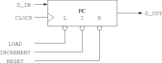 |
Normally, INCREMENT, LOAD, and RESET will be high. When
INCREMENT is low, the PC should increment D_OUT to D_OUT+1 on the rising edge of CLOCK. When LOAD is low, the input
data D_IN should be latched into the register on the rising edge of CLOCK. The system which controls PC will
ensure that LOAD and INCREMENT are never low at the
same time. (In your program, you should have PC do something sensible, like
latch D_IN, if both happen to be low simultaneously.) When RESET is low, PC should immediately reset to  ; it shouldn't
wait for a clock edge. This is normally called a synchronous counter with
synchronous load and asynchronous reset.
; it shouldn't
wait for a clock edge. This is normally called a synchronous counter with
synchronous load and asynchronous reset.
- Design an eight-bit synchronous latch in Verilog.
- Design an eight bit PC as described above in Verilog.
- Write a program which uses the above two designs as functions to
test that they work.
Next: 2 Lab
Up: Lab 8: Registers
Previous: Lab 8: Registers
Copyright © 2008, Electrical Engineering Department, New Mexico Tech
Last Modified 2008-10-29