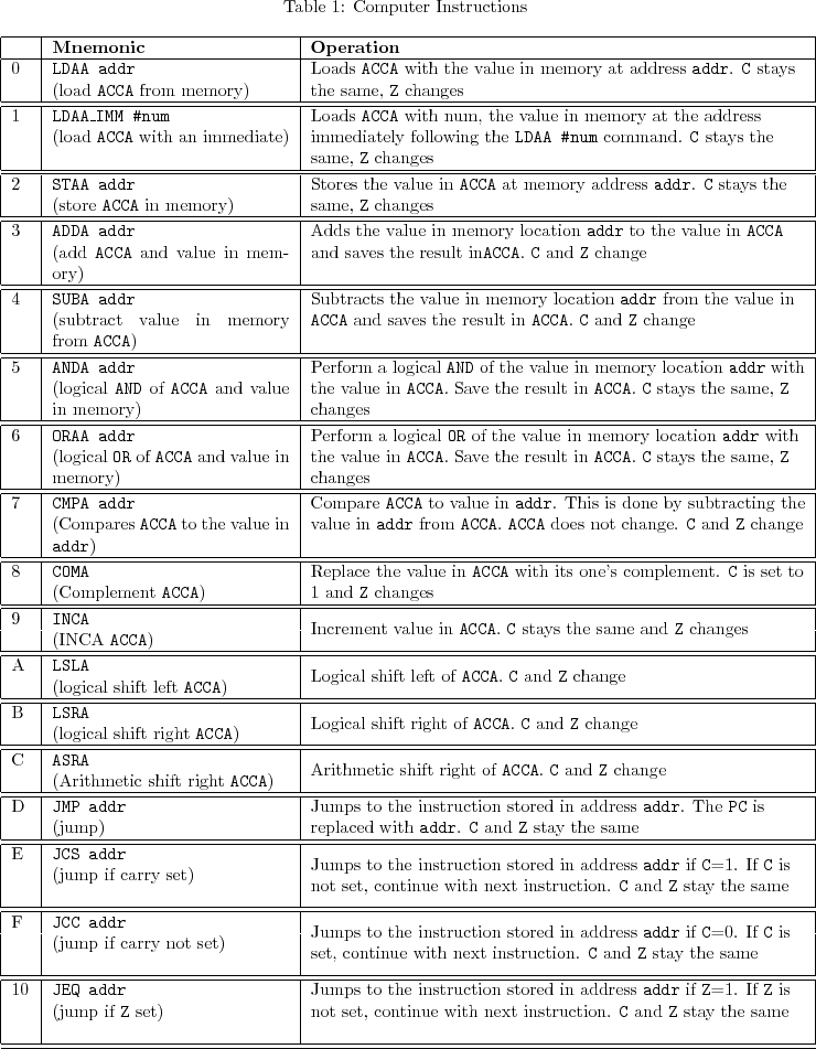
You are on the path do design your first computer. A conceptual block diagram of a simple computer is shown in Figure 1. In previous labs you have already designed the DATA_MUX, the ALU, and required registers. In this lab you will design the computer control unit. The control unit is a finite state machine. Its inputs are the instruction register and the carry, as well as a clock pulse and RESET. The control unit's outputs are the control signals that direct the operation of the rest of the computer. The control unit can be in one of four states: RESET, FETCH, EX1 and EX2:
The outputs of the control unit are the control signals shown on the block
diagram of the computer. Except for ALU_CTRL and MEM_SEL, all
of these signals are active low.
In your
Verilog code you will activate the appropriate signals at the correct times
to implement the instruction the control unit is executing.
During the FETCH cycle the control unit will fetch the next instruction from memory to determine what instruction it should execute. Thus, the FETCH cycle will be the same for all instructions, it will read the instruction from memory, and latch it into the INST register. To do this, IR_LOAD and PC_INC should be low, and MEM_SEL should be set to select the address from the program counter PC. With the control lines set up like this the address to the memory will be from the PC, i.e., the address of the next instruction to execute, and the memory output enable line will be low (active). The memory will put the data at that address on its output lines, which are the input lines to the INST register. On the next clock edge, the data from memory will be latched into the INST register, and the PC will be incremented to the next memory address. What the control unit does next will depend on the data loaded into the INST register. Here is a sample code of how you may structure your module.
| PC | Memory Address | Memory Data |
|
|
80 | 01 |
| 81 | F5 | |
| 82 | Next instruction |
FETCH: During the fetch cycle the instruction register
must be loaded with the instruction op code,
![]() . To do this
the Addr_MUX_Sel must select the PC as the address source,
memory address
. To do this
the Addr_MUX_Sel must select the PC as the address source,
memory address
![]() must be read which causes its value to
be placed on the DATA lines. The value on the DATA lines
must be latched into IR, and the PC must
be incremented. Thus during FETCH you should have PC_INC,
INST_LOAD and Addr_Mux_Sel.
must be read which causes its value to
be placed on the DATA lines. The value on the DATA lines
must be latched into IR, and the PC must
be incremented. Thus during FETCH you should have PC_INC,
INST_LOAD and Addr_Mux_Sel.
| PC | Memory Address | Memory Data |
| 80 | 01 | |
|
|
81 | F5 |
| 82 | Next instruction |
EX1: During EX1, you must read the memory address that
the PC is pointing at. By reading address
![]() the value
0
the value
0![]() F5 is placed on the DATA line. Then 0
F5 is placed on the DATA line. Then 0![]() F5 needs to
be stored in the MAR register. Finally, the program counter should be
incremented. Thus during EX1 you should have PC_INC and MAR_LOAD active, and Addr_Mux_SEL set to PC. After these
steps the situation should be as shown below
F5 needs to
be stored in the MAR register. Finally, the program counter should be
incremented. Thus during EX1 you should have PC_INC and MAR_LOAD active, and Addr_Mux_SEL set to PC. After these
steps the situation should be as shown below
| PC | Memory Address | Memory Data |
| 80 | 01 | |
| 81 | F5 | |
|
|
02 | Next instruction |
EX2: Now that MAR contains the value 0![]() F5, the
multiplexer should select MAR as the source of the address. This
address should then be read which causes the memory contents of address
0
F5, the
multiplexer should select MAR as the source of the address. This
address should then be read which causes the memory contents of address
0![]() F5 to be placed onto the DATA line. Then the ALU can
load this value into ACCA. During EX2 you should have ACCA_LOAD active, Addr_Mux_SEL set to MAR, and ALU_CTL set to LOAD. When the control lines are set up like this,
the value of 0
F5 to be placed onto the DATA line. Then the ALU can
load this value into ACCA. During EX2 you should have ACCA_LOAD active, Addr_Mux_SEL set to MAR, and ALU_CTL set to LOAD. When the control lines are set up like this,
the value of 0![]() F5 will be on the address lines of the memory unit,
and the data lines out of the memory will contain the data in address
0
F5 will be on the address lines of the memory unit,
and the data lines out of the memory will contain the data in address
0![]() F5. This data will be passed through the ALU to the input
of ACCA. On the next clock cycle, the value will be latched into ACCA. Note that you do not want PC_INC active because PC is
already pointing to the next instruction to be executed.
F5. This data will be passed through the ALU to the input
of ACCA. On the next clock cycle, the value will be latched into ACCA. Note that you do not want PC_INC active because PC is
already pointing to the next instruction to be executed.
| PC | Memory Address | Memory Data |
|
|
82 | 02 |
| 83 | F5 | |
| 84 | Next instruction |
| PC | Memory Address | Memory Data |
| 82 | 02 | |
|
|
83 | F5 |
| 84 | Next instruction |
EX1: During the EX1 cycle the PC is pointing at
memory address 0![]() 83. By reading this address, the value 0
83. By reading this address, the value 0![]() F5 is placed on the DATA line. ACCA_LOAD and PC_INC, should be active, MEM_SEL should be set to select PC, and the ALU_CTRL lines should select the function which loads
ACCA. When the control lines are set up like this, the value 0
F5 is placed on the DATA line. ACCA_LOAD and PC_INC, should be active, MEM_SEL should be set to select PC, and the ALU_CTRL lines should select the function which loads
ACCA. When the control lines are set up like this, the value 0![]() 83 will be on the address lines of the memory unit, and the data
lines out of the memory unit will contain the data in address 0
83 will be on the address lines of the memory unit, and the data
lines out of the memory unit will contain the data in address 0![]() 83 (which in this example is 0
83 (which in this example is 0![]() F5. This data will be
passed through the ALU to the input of ACCA. On the next clock
cycle the data will be latched into ACCA. There is no EX2
cycle.
F5. This data will be
passed through the ALU to the input of ACCA. On the next clock
cycle the data will be latched into ACCA. There is no EX2
cycle.
| PC | Memory Address | Memory Data |
|
|
84 | 12 |
| 85 | F5 | |
| 86 | Next instruction |
FETCH: The fetch cycle is the same for this command as it was in Example 1. After the fetch cycle the situation should be:
| PC | Memory Address | Memory Data |
| 84 | 12 | |
|
|
85 | F5 |
| 86 | Next instruction |
EX1: During the EX1 cycle the PC is pointing at
memory address 0![]() 05. By reading this address, the value 0
05. By reading this address, the value 0![]() F5 is placed on the DATA line. ACCA_LOAD and PC_LOAD, should be active, and MEM_SEL should be set to select
PC. When the control lines are set up like this, the value 0
F5 is placed on the DATA line. ACCA_LOAD and PC_LOAD, should be active, and MEM_SEL should be set to select
PC. When the control lines are set up like this, the value 0![]() 85 will be on the address lines of the memory unit, and the data
lines out of the memory unit will contain the data in address 0
85 will be on the address lines of the memory unit, and the data
lines out of the memory unit will contain the data in address 0![]() 85 (which in this example is 0
85 (which in this example is 0![]() F5). This data will
be on the input lines to PC. On the next clock cycle the data will be
latched into PC. There is no EX2 cycle.
F5). This data will
be on the input lines to PC. On the next clock cycle the data will be
latched into PC. There is no EX2 cycle.
![\includegraphics[width=\textwidth]{computer.eps}](img1.png)